
The University of Iowa's DEC PDP-8Restoration Log — early 2026
|
The University of Iowa's DEC PDP-8Restoration Log — early 2026
|
Bug 64: In preparation for an open-house, we decided to start a serious attempt at tuning the memory. We began by investigating the behavior of the memory as we varied the slice voltage. For each slice voltage we tested, we stored 32 consecutive 00008 in memory starting at address 60008 and then examined memory to see how many values were still zero, and then we stored we stored 32 consecutive 77778 to see how many values were still all ones.
| Voltage | not 0000 | not 7777 |
|---|---|---|
| 7.7 | 32 | 0 |
| 7.68 | 19 | 0 |
| 7.62 | 17 | 0 |
| 7.6 | 13 | 0 |
| 7.56 | 0 | 0 |
| 7.5 | 0 | 13 |
| 7.54 | 0 | 13 |
| 7.4 | 0 | 15 |
| 7.1 | 0 | 32 |
The slice voltage was adjusted by turning the topmost trimmer on the G008 Master Slice Control board. In adjusting this and other Bourns TrimPot trimmers on DEC flip-chip modules, we have observed that the voltage is quantized, changeing in discrete steps as the trimmer screw is turned. We wonder if the trimmers are wire-wound with a contact brush touches one turn at a time.
The voltage readings here were eyeballed off of an analog meter, so the accuracy is probably 0.02V at best.
What is clear here is that the memory only just barely works. We were hoping to find a range of slice voltages that worked and then set the potentiometer to the middle of the working range.
The working range is probably a 3-dimensional volume, with the dimensions being
The next memory tuning exercise will involve playing with the other two dimensions.
With memory working as best we could adjust it, we loaded demo code in memory for the open house on Jan 20-22:
Some of the above were hand-relocated to run in new memory locations. All were tested and seemed to work.

|

|
Eliminating the bare wire jumper on the transformer reduces the hazards posed
by this power supply, but it would be nice to make a sheet metal cover over
the transformer comparable to the transformer covers on the Type 779
transformers. This will require some sheet metal bending.
Bug 80: During a demo, after turning off the Teletype, when we turned it on again, the motor did not spin. It buzzed, and when you turned the fan, you could feel it vibrating. This implies that there is power to the motor. It is a capacitor start motor with a starting relay. Teletype's schematic FS-10 MOTORS documents this and several other motor options. Any of the following could cause the motor not to spin despite there being power to the motor:
We pulled the quick-connect connectors to the starting relay, allowing us to use an ohm-meter to verify that the primary motor windings is 9Ω and the starting winding is 16.5Ω ruling out a burnt-out motor winding. Measuring between the primary and starting widings, have 25.5Ω, so there are no shorts between the windings.

|

|
The relay is a normally open relay with an approximately 0.1Ω coil. During the motor's starting surge, the relay closes to power the starting winding. Once the motor is up to speed, the current through the primary motor winding is too low to hold the relay closed. Aside from evidence of contact arcing, the relay is in good condition. We burnished the contacts and put the relay back. We did not make any changes to the adjusting screw (the screw on the left of the right photo with a red dot of paint on it).
After reassembly, we used an ohm meter to verify that the start relay closes when power is briefly applied to the motor.
The above observations point to the motor start capacitor itself. Teletype's schematic identifies this as C3 88-108, which agrees with the markings on the capacitor, 88-108MFD. This is an 88-108μF capacitor, a very common value of motor start capacitor.
Bug 80: Continuing the diagnostic work from Jan 22, we used an analog ohm meter on the Rx1K scale to test the 88-108μF motor-start capacitor. It conducts very briefly when the meter leads are first connected and then drifts up to infinite resistance. That is how a capacitor ought to behave when measured this way. We compared it with a known good 5μF capacitor, and saw that the response on the ohm meter was far stronger with the latter than with the capacitor from the Teletype. Therefore, while the capacitor still has some capacity, it has much less than 5μF.
So, we ordered a replacement capacitor. The original capacitor was a 1" (26mm) diameter cylinder 2.5" (65mm) long. The smallest replacement we could find was 34mm by 69mm, 8mm larger in diameter. This will be a tight fit in the space in the Teletype. Also, we will need some 4.8mm (0.187") faston connectors to attach the capacitor to the wiring. Teletype corp. seems to have used that size exclusively, while the similar connectors in the PDP-8 are all the more common 1/4" wide.
|

|
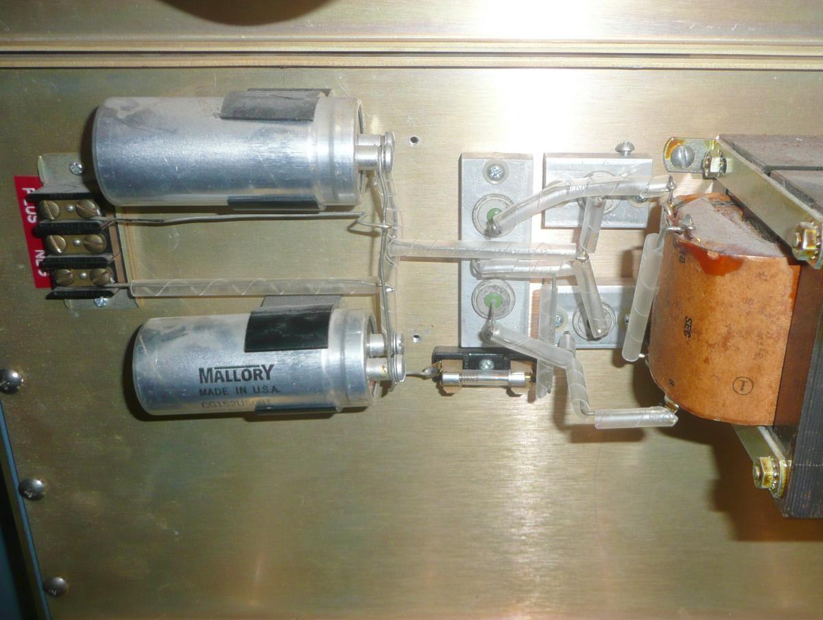
We had finished rewiring the transformer primary. Now, we rewired the secondary, moving the fuse to the bridge between the two secondary windings and finishing adding spiral-wrapped insulation to the remaining uninsulated wires.
We still need to install metal shields to protect fingers and make accidental
shorts less likely. This is most important on the 120V primary side of the
transformer, but would also be helpful on the 30V secondary side.

|
Bug 64: We returned to the memory tuning problem last addressed on Jan. 14. We connected the current probe and began trying to adjust the inhibit and read-write (or select) currents. We found that the inhibit current was 0.28A, not the recommended 0.31A. We were able to bring it up to 0.295, but no higher.
We also found that the select current was also low. We were able to turn it up to 0.32A.
With these changes, we repeated the exercise we had done on Jan. 14, varying the slice voltage, and at each step, writing 16 consecutive words of 00008 and 16 consecutive words of 77778 to memory and reading them back. On Jan. 14, only one slice voltage worked, 7.56V. Our changes to the select and inhibit currents made a big difference:
We left the slice voltage set to 7.72V, roughly the middle of the good range.
|
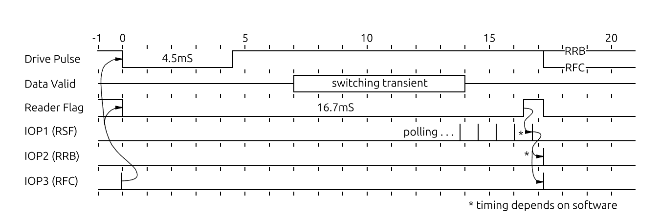
The 16.7mS delay between initiation of a read cycle and the setting
of the device flag allowing initiation of the next cycle is also from the
Tally manual. The role of the RSF, RRB and RFC
instructions and their relationship to the reader flag and the rest of the
read cycle is from the description of the Type 750 High Speed Reader
interface on
pages 62-63 of the
PDP-8 Users Handbook,
Digital Equipment Corporation, F-85, 5/66, 1966.
From this timing diagram, we conclude that our speculation on
July 1, 2025 that only 2 delays
are required seems correct so long as the reader flag is only set
after the full 16.7mS read cycle, at the earliest time that it is acceptable
to start the next read cycle. Given that software should only take a few
tens of microseconds to initiate the next read, this should not appreciably
slow the reader. It would be possible, at the cost of considerable complexity,
to read the input into the reader-data register and set the reader-ready flag
at the end of the switching transient, 14mS into the read cycle. This would
require an additional delay and an additional flipflop to allow the
RFC to queue up starting a read cycle before 16.7mS have elapsed.

|

|
So, we hunted for new parts. While 88-108μF capacitors are available, they tend to come in large packages. The smallest motor start capacitors we could find were CD60 100μF &plusminus; 15% rated at 250VAC. Among these, we found some with bodies 34mm diameter by 69mm or 70mm long with wire terminals comparable to the originals. Most modern motor starting capacitors are polyester film and not electrolytic capacitors, and we think this applies to the capacitor we bought.
Polyester film capacitors are generally larger than electrolytics, and in this
case, the difference in size is enough that we were not certain that the
new capacitor would fit. As can be seen in the photos here, the new
capacitor just fits. We had to bend the hold-down finger that extends from
the starting relay mounting bracket to make it fit, and there was just over
1mm clearance between the new capacitor and the fan on the back of the Teletype
motor. Fortunately, the capacitor is tightly held and does not threaten to
bounce into the fan, and as the photo shows, the fan spins freely and the
Teletype works well.
Bug 16: Now that the homebrew reader-punch power supply works and our estimate of power demand made on Dec. 11, 2025 suggests that it will not overtax the PDP-8's rack wiring, we jumpered it to the line-line current terminal strip on the Type 779 power supply directly below it.
Bug 10: We have not powered up the Type 779 supply since Oct. 9, 2014 so we disconnected the fan in the base of the I/O rack and disconnected the wiring from the supply to the logic in the rack and then connected it to a variac so we could slowly raise the voltage.
The ferroresonant transformers in the Type 779 supply created a very nonlinear relationship between the output voltage and the setting on the variac. Under no load, the DC output voltages on the Type 779 supply approached their rated values at AC input voltages under 50 volts. Fortunately, the capacitors we had reformed a decade ago were in pretty good shape, and we saw no ill effects from raising the output voltage in 5V steps about an hour apart.
We paused periodically to check for leakage by looking at the rate of decay of the charged capacitors with no power input and no load. We were briefly alarmed to discover that the +10 output of the Type 779 supply was decaying rapidly, until we noticed that there is a 15Ω resistor shunting a 35,000μF capacitor to ground for that output. output to ground. This matches the Type 779 Power Supply schematic. The RC time constant for this capacitor is 35,000μF×15Ω = 0.525s. By eyeball, watching the needle of an analog volt meter drop as we turned off the power, it fell most but not all of the way to zero in about a second, which is in the right order of magnitude for this RC time constant. We conclude, therefore, that the supply is good.
Note:
Ferroresonant transformers
are well known to hum louder than other transformers, and in our Type 779
supply, we noticed this hum, starting when the AC input was around 30V and
getting louder as the AC input was ramped up to 120V.
Bug 43: With memory working better, we tried keying in a more ambitious program from the front panel. Of course, we made mistakes in the code and mistakes in the keying in. We debugged the code using a Linux-based assembler and PDP-8/E emulator before trying again. The following code worked:
           / Teletype demo (poorly optimized code)
           / Typing char echos and appends char to buffer except
           STX=    202             / Control B -- clear buffer
           ENQ=    205             / Control E -- replays buffer
           *4000
04000 7200         CLA
04001 1253         TAD     PBUF
04002 3260         DCA     INPTR   / bufptr = start
           LOOP,                   / loop -- outer loop of program
04003 6031 INPOLL, KSF             /    loop -- polling input
04004 5203         JMP     INPOLL  /    until -- key pressed
04005 6036         KRB
04006 3256         DCA     CHAR    /    char = character from tty
04007 1256         TAD     CHAR
04010 1254         TAD     NEGSTX
04011 7440         SZA             /    if char = STX
04012 5216         JMP     NOTSTX
04013 1253         TAD     PBUF
04014 3260         DCA     INPTR   /       bufptr = start
04015 5203         JMP     LOOP    /       continue
04016 7200 NOTSTX, CLA             /    endif
04017 1256         TAD     CHAR
04020 1255         TAD     NEGENQ
04021 7440         SZA             /    if char = ENQ
04022 5242         JMP     NOTENQ
04023 1253         TAD     PBUF
04024 3257         DCA     OUTPTR  /       outptr = start
04025 7200 OUTLP,  CLA             /       loop -- exit by break
04026 1260         TAD     INPTR
04027 7041         CMA IAC
04030 1257         TAD     OUTPTR  /          a = outptr-inptr
04031 7500         SMA             /          if a >= 0
04032 5203         JMP     LOOP    /             break
04033 7200         CLA
04034 1657         TAD I   OUTPTR
04035 6046         TLS             /          output *outptr
04036 6041 OUTPOL, TSF             /          loop
04037 5236         JMP     OUTPOL  /          until output done
04040 2257         ISZ     OUTPTR  /          outptr++
04041 5225         JMP     OUTLP   /       endloop
                                   /       continue outer loop
04042 7200 NOTENQ, CLA             /    endif
04043 1256         TAD     CHAR
04044 3660         DCA I   INPTR   /    *inptr = char
04045 2260         ISZ     INPTR   /    inptr++
04046 1256         TAD     CHAR
04047 6046         TLS             /    output char (echo it)
04050 6041 OUTPOM, TSF             /    loop
04051 5250         JMP     OUTPOM  /    until output done
04052 5203         JMP     LOOP    / forever

           / constants
04053 4061 PBUF,   BUF             / start of buffer
04054 7576 NEGSTX, -STX            / used to compare with stx
04055 7573 NEGENQ, -ENQ            / used to compare with enq

           / variables
04056 0000 CHAR,   .-.             / most recent input character
04057 0000 OUTPTR, .-.             / buf pointer to output buffer
04060 0000 INPTR,  .-.             / buf pointer fill buffer
04061 0000 BUF,    .-.             / start of data buffer
This is a far more satisfactory Teletype demo program than the smaller one we keyed in on Sept. 29, 2025 (that code was still in memory).
With this demo code working, we tried using the RIM loader to load the BIN loader. This seemed to work, but when we tried using the BIN loader to load ODT, the octal debugging tool, it did nothing. Obviously, we need to explore what went wrong. The paper tapes we used were marked as follows, on adhesive labels that fell off until we re-glued them:

|
With our wrench made, we were able to tighten the marginally loose screws in the drive-link. These had been slightly loosened at some point in the past while trying to adjust the drive link. We solved the actual linefeed problem by careful adjustment of the drive-link up stop.
Bug 81: Trying the Teletype demo program, it stopped working. Specifically, when we typed ABCDEFG it echoed CBCFGFG. First, since we were using our demo program, we looked at the accumulator where each input character goes (until you type the next one). That was correct. So we made a table of what was typed and what was printed:
| Typed | Printed | ||
|---|---|---|---|
| A | 1000001 | C | 1000011 |
| B | 1000010 | B | 1000010 |
| C | 1000011 | C | 1000011 |
| D | 1000100 | F | 1000110 |
| E | 1000101 | G | 1000111 |
| F | 1000110 | F | 1000110 |
| G | 1000111 | G | 1000111 |
Teletype numbers bits from the least significant bit, bit number 1. In those terms, the problem is clear from the above table. Bit 2 is stuck at 1 in the receive mechanism in the Teletype.
Looking there, we found that the bit-2 blocking lever seems to hang in the up position. Why? We were unable to figure this out.
Bug 81: We had to remove the carriage-return dashpot from the Teletype (part number 181193) in order to get a better view of the 8 blocking levers (part numbers 180643 and 180644). With the dash pot out of the way, we could rock the blocking levers, pushing down on the tail of the lever with one probe and pushing down on the head with the other. Lever 1 rocked freely, but lever 2 was interfering with something.
When down, each blocking lever blocks a tooth on the corresponding code bar that represents one bit of data in the mechanical data bus that runs under the carriage and out to the paper-tape punch. (The code bar for bit 2 is part number 180933. The relationship between code bars and blocking levers is shown in the Maintenance Manual, Vol 2, page 39.) If the code bar motion was just shy of enough to allow the blocking lever to fall freely, this could explain the problem. The adjustment for that is documented in the Maintenance Manual, Vol. 2, page 36, and is really ugly, requiring removal of the motor. Fortunately, the manual also inicated a simple test for this problem, pressing back on the code bars. This test showed that this was not the problem.
The keyboard end of the blocking levers sits under the blocking-lever upstop (part number 180682), this blocked our view of that end of the levers, so we removed it. At this point, we were finally able to see that the tip of the blocking lever was rubbing in the slot in the comb that holds the levers in alignment. This comb is on the top of the left end of the front tie bracket (part number 180950),
The space in this comb for blocking lever 3 was a bit wider than the space for lever 2, so we hypothesized that the space for lever 2 was binding on the lever. The test was simple. We rested the tip of a probe on the left side of the comb tooth and gently bumped it with a finger. The goal was to bend the tooth just slightly. Amazingly, this worked!
|
In cleaning up the wiring on the backplane, we found that the 30V power to the
reader was delivered by 18AWG wires that snaked from the power supply around to
wirewrap pins on the backplane, where they were soldered. This was ugly, at
best. We decided that the best way to bring power to this interface would be
through the Flip-Chip board serving as a cable connector to the reader.
From there, backplane wiring can deliver power to the W043 (or W040) solenoid
driver.
| ||||
|
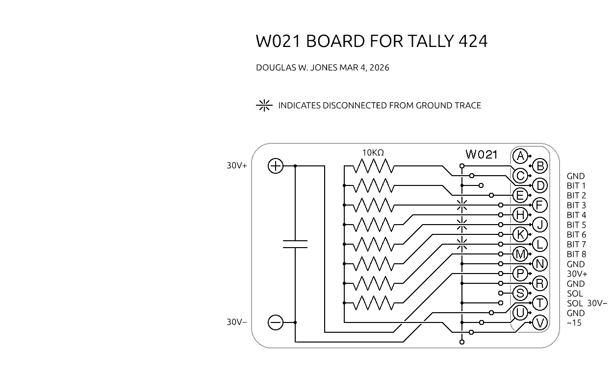
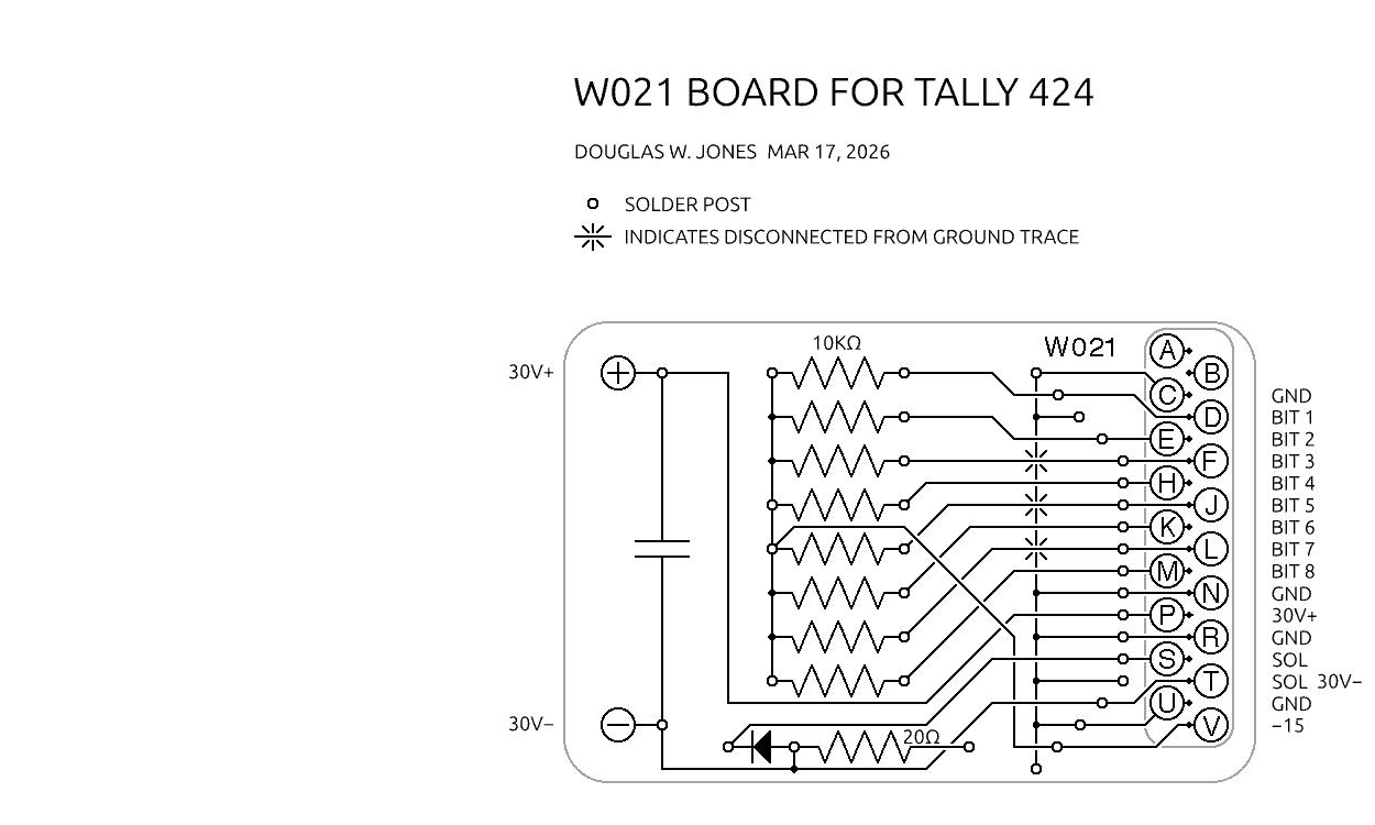
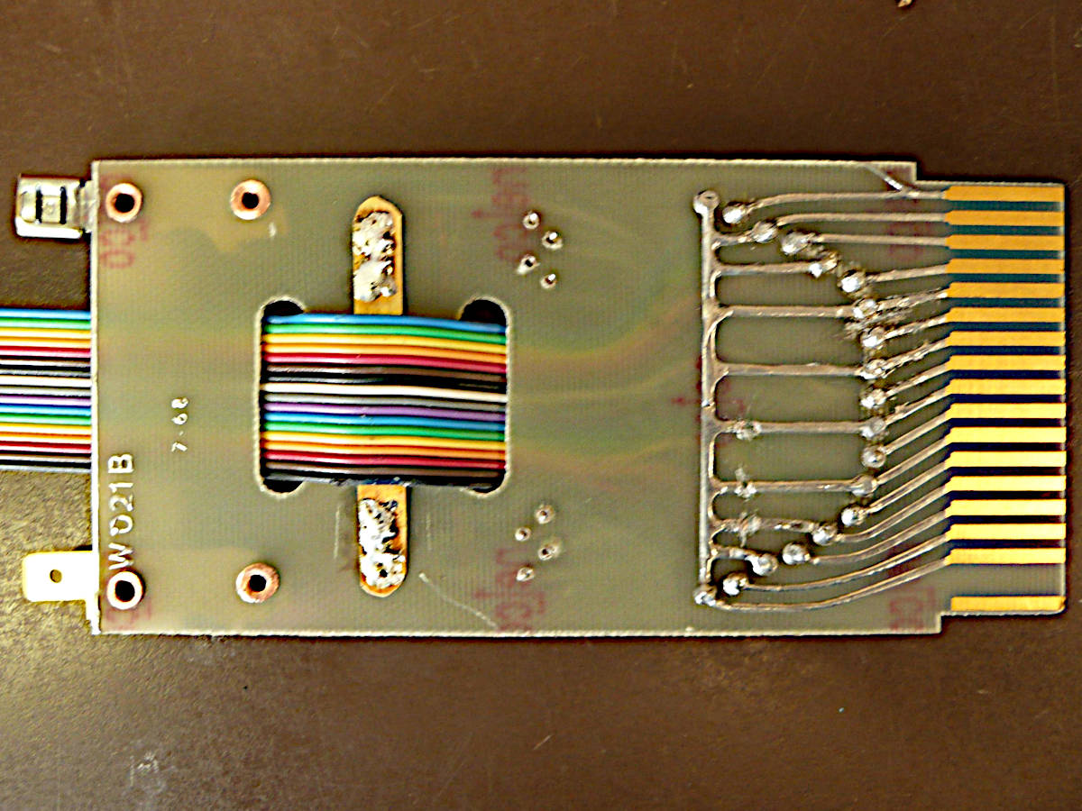
One obvious change we need to make is to move the pull-down resistors that are currently soldered to backplane pins somewhere else. The obvious place to move them is onto the cable connector. This move requires that -15V power be provided to the connector. Unfortunately, the W021 boards we have (DEC's go-to board for connecting cables to the backplane) does not provide connections to pins A or B, the +10 and -15 supply lines. We decided to use pin V for this purpose, as it is not currently connected.
A second problem is where to bring in the 30V power. Pins S and T are currently wired to run the tape-advance solenoid, pins R and U are grounded in the stock W021 board, leaving pin P as a candidate to carry the +30 supply. As wired by the psychology department, this was grounded at the W021 board, but this ground connection should really be as close to the solenoid drivers as possible. Therefore, we opted to put this connection on the unused pin P, between the grounded pins N and R. The -30 connecton will directly power one side of the solenoid, just as it did in the psych. department version.
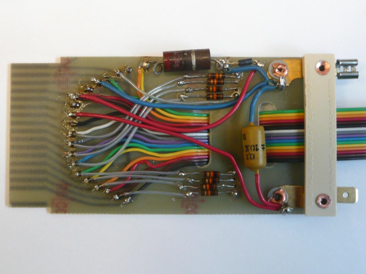
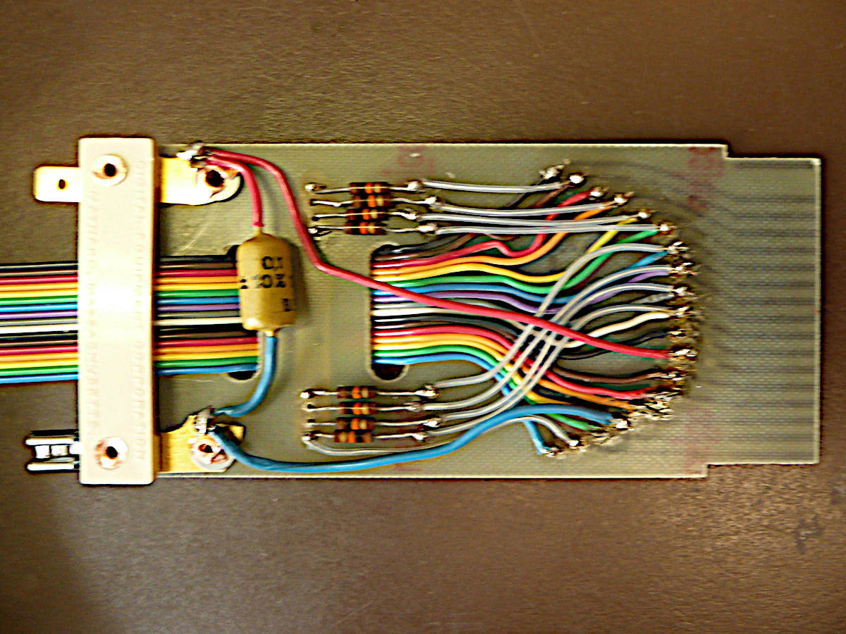
Bug 12: After working out these details, we removed, salvaged and tested the 8 pull-down resistors from the backplane, cut 3 of the factory ground connections on a W021 board and soldered the ribbon cable in place. Our plan is to put 1/4" Faston tab connectors on the back corners of the board for power connections and to mount the resistors above and below the cable. Dec recommends putting a capacitor across the 30V power if the wire from the power supply is longer than 3 feet, so we will put this on the board as well.
| ||
|
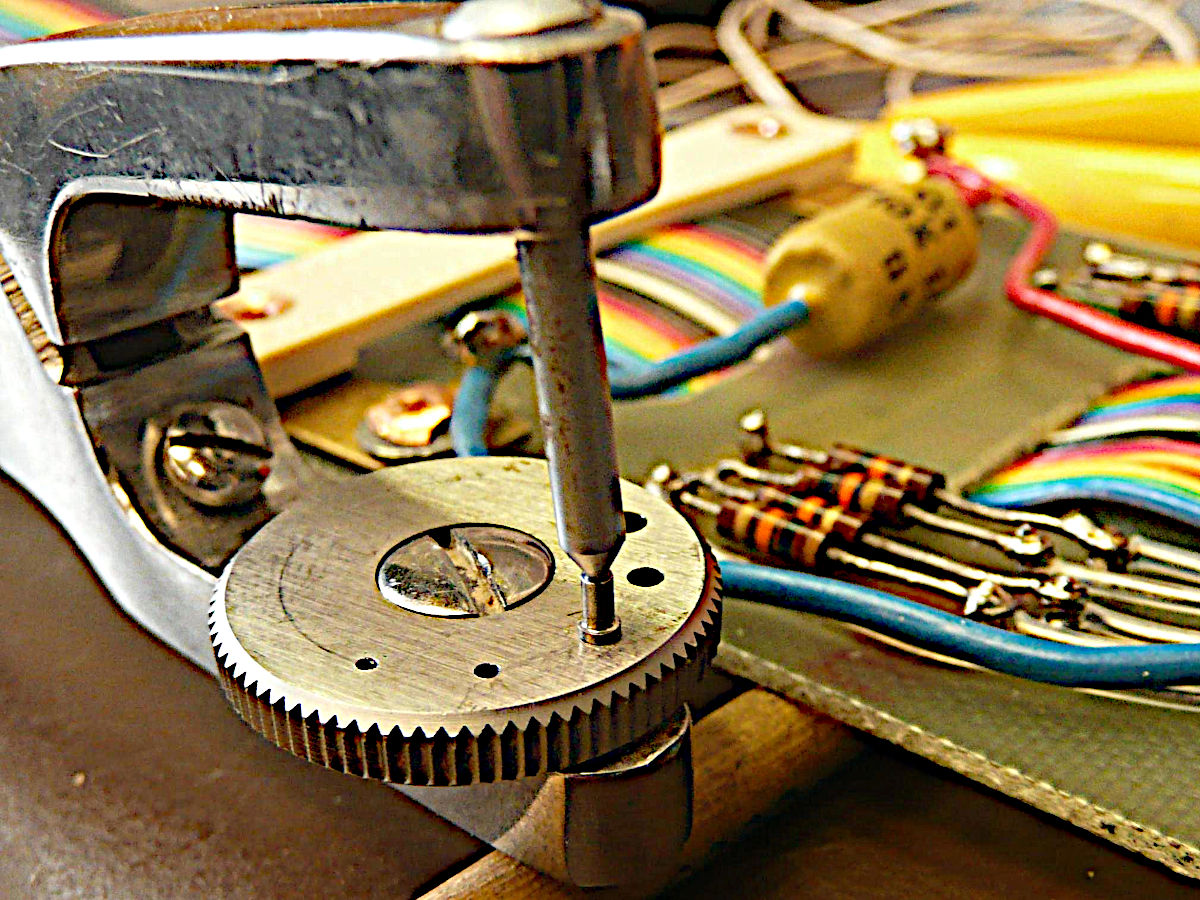
We drilled out the rivets holding the cable strain relief and used them to attach 1/4" faston connectors to the two back corners of the board. DEC did the same thing on G850 motor driver boards. As on the G850, we used two rivets to hold each connector, with one also holding the cable strain relief and one to prevent the faston connector from pivoting.
The faston connectors on the G850 are both male, but this is an AC controller,
where mis-connecting the power would cause no damage. Our application is for
DC, so we used polarized connectors, one male and one female.
|
We used a brass strip to link the row of posts at the -15V end of the resistors. We had hoped to put in a row of 8 posts into this strip, but we drilled the holes too to use our dental tool to rivet the posts so we only used 4 posts. The posts rivet the brass strip in place, and we used through-hole mounting for the other 4 resistors.
We used the resistors we had unsoldered from backplane slot B32 on Mar. 5. For a photo of these resistors prior to salvage, see the log entry for July 1, 2025.
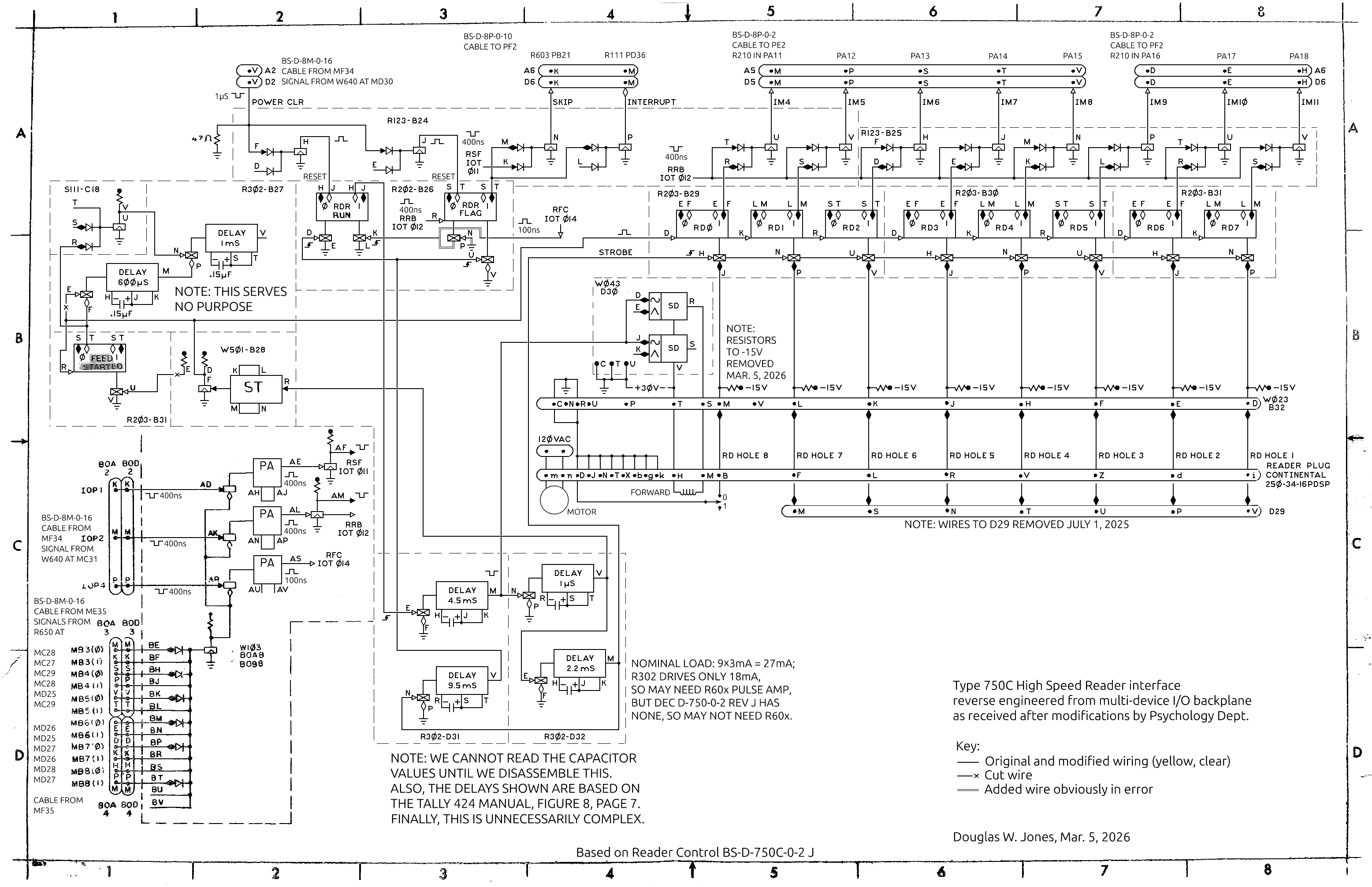
Bug 34 and Bug 82: We removed a number of wires from the Type 750C High Speed Paper Tape Reader interface part of the I/O backplane. Most of these wires were added by the Psychology department as part of their modificaiton of the intrface, insulation colors other than yellow. We also removed cut wires and wires with no obvious function, according to our annotated reverse engineering diagram given in the log entry for Feb. 25.
In the process, we found some errors in this diagram, and we learned some things:
With regard to the data inversion, The tape reader can produce either polarity of data, depending on how the cable connector is wired (See page 8 of the Tally 424 manual, which is page 39 in the Archive PDF). we hypothesize that the psychology department wired the cable incorrectly, discovered that all the data was inverted, and solved the problem by re-inverting the data at the flipflops instead of fixing the cable.
This leads us to a question: Do we keep Psychology's changes to the
interface and build our new cable to match, or do we restore this part of
the interface so it conforms to DEC's documentaiton and build the cable
that Psychology ought to have made?
| |||
| |||
|
There is no clear reason to use a Zener diode where this diode was wired into the circuit, and a 22V Zener diode across an inductor driven at the rated 24V almost guarantees diode failure. We opted to replace this diode with a 1N4003 we had on hand. This makes sense in this context.
Moving the resistor and diode onto the cable connector makes the Tally reader more closely conform to the schematics given on page 8 of the Tally 424 manual, which is page 39 in the Archive PDF. Exact conformity is not possible because our reader does not have a coil on its reverse solenoid. Placing the pull-down resistors and snubber circuitry on the modified W021 board is in the spirit of what DEC did with their W070 Teletype Connector board.
There was just space along the lower margin of our W021 board to mount these
parts, using 3 new solder posts to support them. The photo here
shows the result.
Bug 43: On Feb 19 we had tried to run the BIN loader and it failed to load a program. One thing we know about BIN is that is uses subroutine calls, and the PDP-8 JMS instruction is one of the more complex instructions on the machine. We wondered if there might be a problem with JMS, so we wrote a small diagnostic and keyed it in:
           *0100                   / worked in page 0
           *0300                   / could not load in page 1!!!
           *0500                   / worked in page 2
00500 7200 START,  CLA
00501 7421         MQL             / start at zero iterations
00502 7200 LOOP,   CLA
00503 1322         TAD     WHLT
00504 3307         DCA     T       / setup for stop 2
00505 4307         JMS     T
00506 7402 RET,    HLT             / stop 1 if JMS doesn't jump
00507 0000 T,      .-.             / stop 2 if JMS goes to T, not T+1
00510 7440         SZA
00511 7402         HLT             / stop 3 if JMS changed AC
00512 1307         TAD     T
00513 1323         TAD     NRET    / check return addr
00514 7440         SZA
00515 7402         HLT             / stop 4 if wrong return addr
00516 7501         MQA             / count iterations to
00517 7001         IAC             /   differentiate intermittent
00520 7421         MQL             /   and solid failures
00521 5302         JMP     LOOP
00522 7402 WHLT,   HLT             / halt instr used for stop 2
00523 7272 NRET,   -RET            / compare this with return address
           $
As indicated in the comments, this code worked when keyed in starting at 01008, which is the middle of page 0. The program does not use JMS to call a subroutine, instead, it checks to see that JMS does everything advertised, halting if JMS does not jump, tries to execute the destination location, alters the accumulator, or fails to store the correct return address. It uses the MQ register to count iterations in order to help identify intermittent failures. This program ran for several minutes, making us fairly sure that JMS worked with page 0 addressing mode.
When we reassembled it and keyed it in starting at 03008, the middle of page 1, it did not work, and on investigation, we found that it was not even in memory in page 1. We had hoped to use this test to see if JMS worked when using current-page addressing.
When we reassembled it and keyed it in starting at 05008, the middle of page 2, it worked as well as it had in page 0, verifying that JMS works correctly with current-page addressing.
Bug 64:
This leads us to hypothesize that the problem is in memory.
Do we have a problem using odd-numbered pages? That would certainly make it
difficult to load large programs. We need to investigat this.
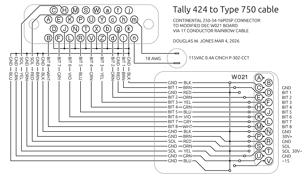
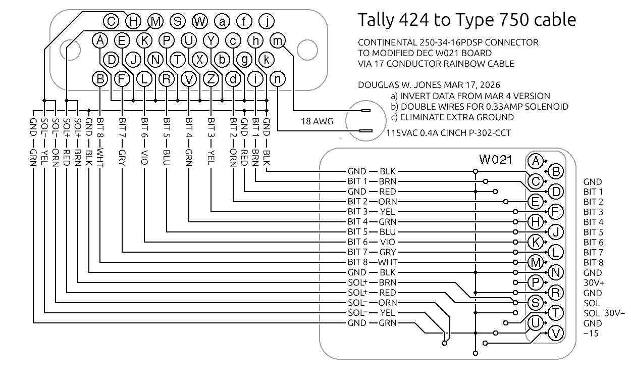
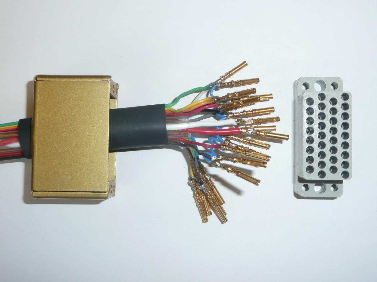
Bug 12: We began work on the paper tape reader end of the cable. According to the Tape Reader Manual - Model 424, Tally Register Corporation, Seattle, no date (Revised 4-1-62), page 6, the tape reader has a Continental #250-34-16PDSP 34-pin plug. We verified this, and we found that compatable connectors are available from numerous manufacturers, primarily because they are used for ITU V.35 modems. These connectors are expensive, but we found an old cable in a junk bin and salvaged the contacts, shell and connector body. The one we found was a Positronic GMCT34F that we empirically verified could mate with the connector on the Tally reader.
|
Before starting work, we slipped a piece of heat-shrink tubing over the ribbon
cable and power cable, and slipped the connector shell over that.
We then
soldered the contacts to the wires in the ribbon cable, one contact per wire,
one contact for each pair of wires carrying power to the tape-advance
solenoid in the reader, 8 contacts jumpered together for the 4 ground wires
in the cable, and 1 contact on each of the 2 120VAC wires for the motor.
All of this was done before any contacts were inserted in the connector block.
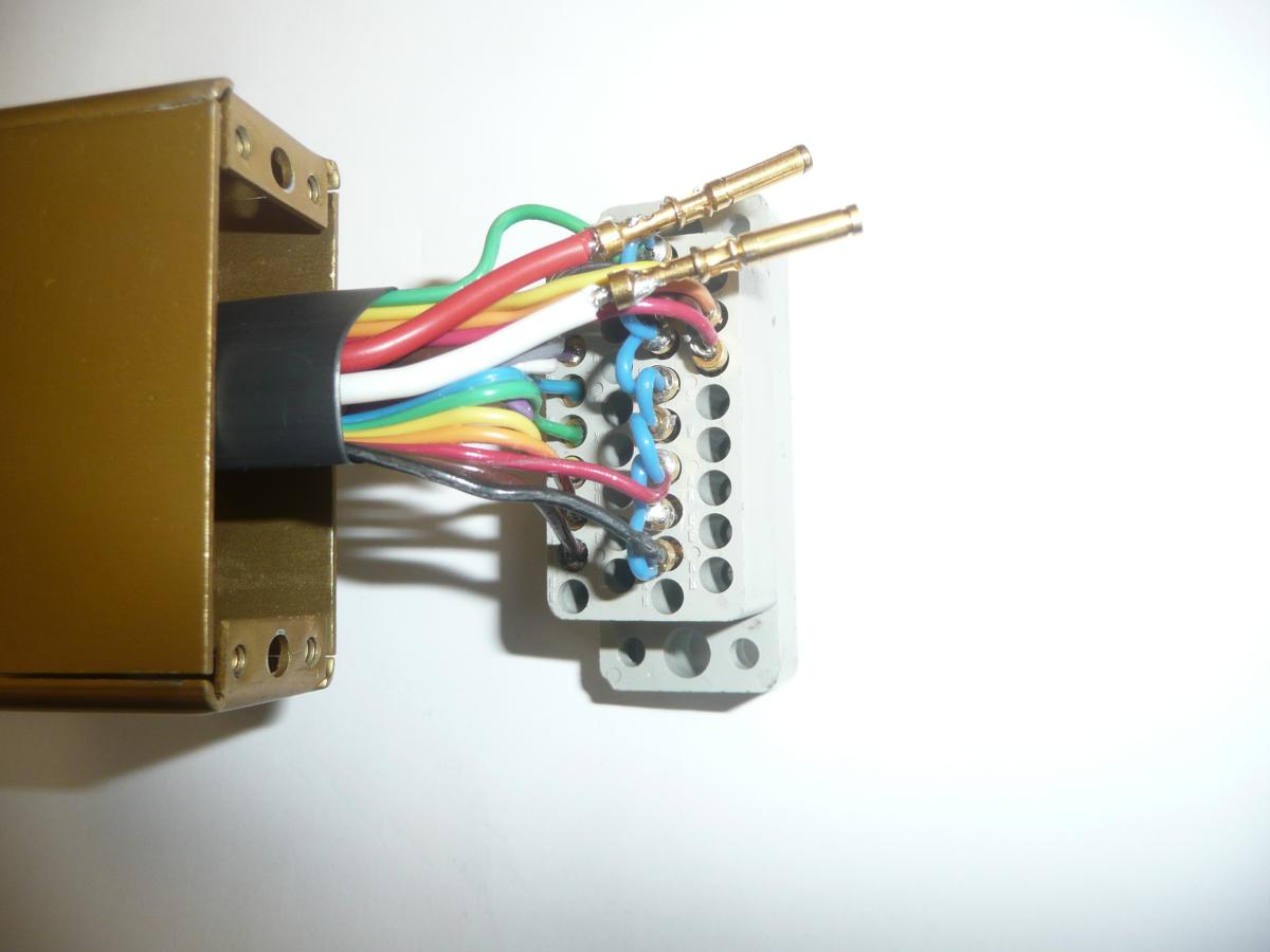
The result resembled an explosion of gold-plated contacts at the end of the
cable, as shown in the first photo.
|
|
Bug 13:
The remaining job is to rewire the controller and wire a 120VAC
power connection for our cable.
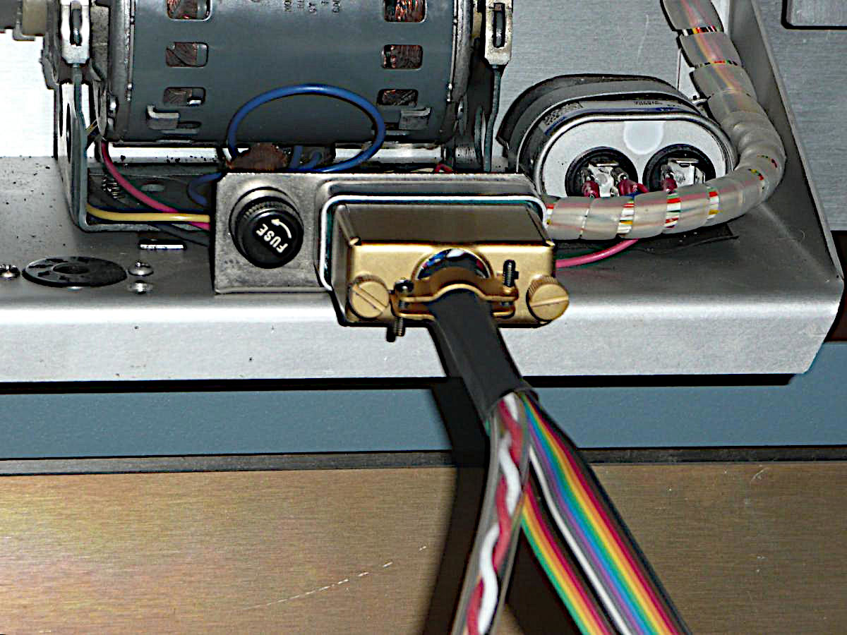
Bug 13 and Bug 16: We added wiring to bring line power to the cable for the Tally 424 paper-tape reader that we finished on Mar 26. DEC used red-white twisted pair for 120V power distribution, so used the same. The addition was about a foot long, from a Jones plug that mates with the cable from the reader to the terminal strip at the back of the I/O rack.
Bug 64: On Mar 24 we observed that we had found half a page (64 words) of memory that did not work, starting at address 03008, the middle of page 1.
We wrote the following memory diagnostic program:
           / Little memory tester, tests all but low page 0
           / tests each location with 4096 possible values
           / does not disturb existing memory contents
           / show bad addresses in MQ.
           / if SR==0, tests just one word then halts
           / continue from halt picks up at next word
           *0020
00020 7200 START,  CLA             / forever do
00021 1056         TAD     MSTART
00022 3053         DCA     MLOC    /   mloc = mstart
00023 7421         MQL             /   MQ = 0
           NEXT,                   /   for most of memory -- AC == 0
00024 1453         TAD I   MLOC    /     -- save value for later
00025 3054         DCA     MSAVE   /     msave = *mloc
00026 3055         DCA     MVAL    /     mval = 0
           RETEST,                 /     for all values -- AC == 0
00027 1055         TAD     MVAL
00030 3453         DCA I   MLOC    /       *mloc = mval
00031 1453         TAD I   MLOC
00032 7041         CMA IAC
00033 1055         TAD     MVAL
00034 7450         SNA
00035 5041         JMP     OK      /       if *mloc != mval
00036 7200         CLA
00037 1053         TAD     MLOC
00040 7421         MQL             /         MQ = mloc -- show addr
           OK,                     /       endif -- AC == 0
00041 2055         ISZ     MVAL    /       mval++
00042 5027         JMP     RETEST  /     endloop
00043 1054         TAD     MSAVE   /     -- restore original value
00044 3453         DCA I   MLOC    /     *mloc = msave
00045 7404         OSR
00046 7650         SNA CLA
00047 7402         HLT             /     if SR==0 halt -- AC == 0
00050 2053         ISZ     MLOC
00051 5024         JMP     NEXT    /   until end of memory -- AC == 0
00052 5020         JMP     START   / forever
00053 0000 MLOC,   .-.             / addr being tested
00054 0000 MSAVE,  .-.             / save value that was in *mloc
00055 0000 MVAL,   .-.             / value used for testing
00056 0057 MSTART, .+1
           $
When we ran this diagnostic, it showed 16 half-page (64 word) blocks of memory that were defective. Defective addresses had the form These addresses all involve bits 3-5 of the memory address (remember that the 12 bits in a PDP-8 word are numbered starting at the left).
We reviewed the documentation for the PDP-8 memory address decoding, and found Drawing BS-D-8M-0-12 in the PDP-8 Maintenance Manual, F87, Digital Equipment Corp., 1966. This drawing shows that bits 3 to 5 of the memory address are decoded by four G209 memory select drivers in backplane slots MD6 through MD9.
Before looking at any details of how the memory select drivers work, we tried an experiment, swapping the driver in slot MD6 with that in MD8, and swapping MD7 and MD9. Before this swap, the problem addresses were of the form x3xx8 or x6xx8. After the swap, the problems moved to x2xx8 or x7xx8.
This experiment convinces us that the problem is in one of these 4 boards and not in the core memory itself. This is good news. Repairing a problem in the core array would be very hard, while repairing boards is fairly simple, once the problem is isolated.
To further isolate the problem, we tried switching the boards in MD6 and MD7.
This broke our diagnostic! Hand testing using the front-panel switches showed
that the problem had moved to the memory addresses where we had our code.
We immediately swapped the boards back, but it seems that we will have to
re-load our code before continuing.
We quit for the day at this point, being fairly sure that the problem board
is one of the two in slots MD6 and MD7. The obvious next experiment will be
to switch MD7 with MD8. If that moves the problem, we can be fairly sure
that the problem is in the board currently in MD7.
|
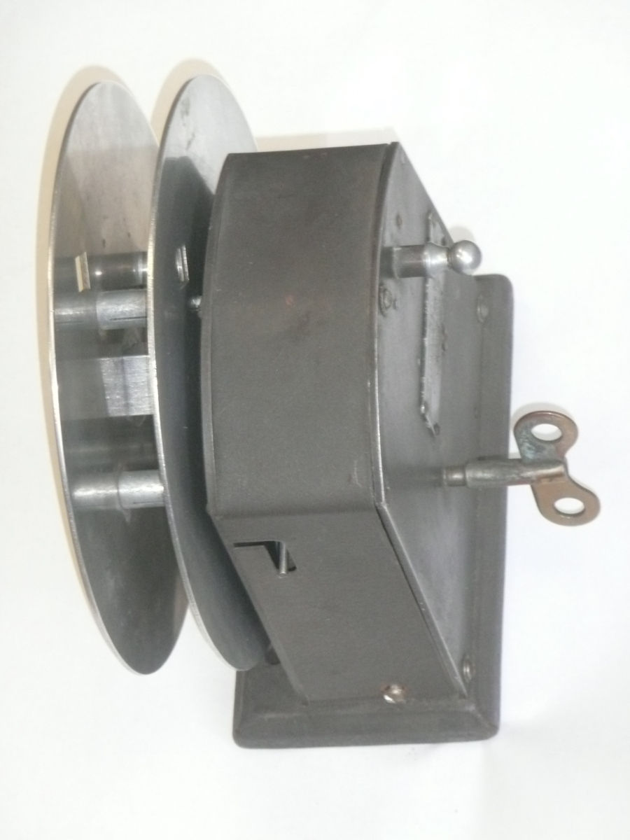
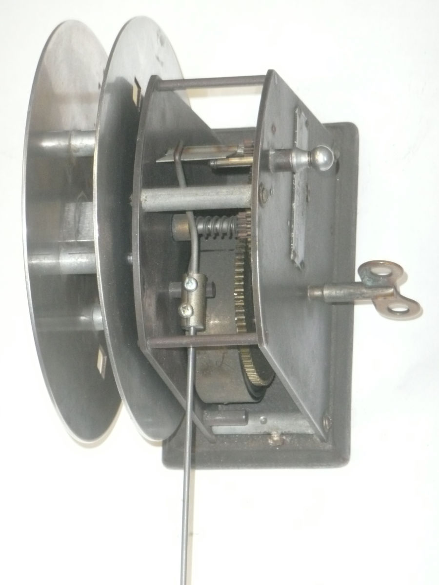
The cut-off stub of the arm is made of 3/32" steel music wire, evidently welded to its pivot. There is space in the winder housing for a splice 3/4" long and 3/8" in diameter to mate a new arm to the cut off stub.
Bug 84: The other problem we noted with the tape winder was that the take-up reel only holds 7/8" 6-bit tape. While our winder has a plaque indicating that it was sold by Fairchild, a quick examination of the bottom of the third page of the J. H. Bunnell & Co. catalog shows that this winder is identical to the Bunnell Type 3-1 winder, and that our reel is what the 4th page of the Bunnell catalog calls a ball-lock reel. Bunnell made this reel for many different tape widths, including the 1" width used for the 8-bit tape used by our PDP-8.
Bug 85: We have only a limited supply of Teletype paper. New-old-stock paper is becoming increasingly difficult to obtain, but the web site qrpbuilder.com suggests using 8.5" glossy headrest paper (antimacassar paper). This paper is used to line the headrests of medical exam tables, and as the University of Iowa has a huge hospital, it should be stocked on campus.
Headrest paper comes on 225' rolls and the primary incompatability with Teletype paper is that the paper roll support on a Teletype is designed for a core tube with a 1" inside diameter, while headrest paper is wrapped on cores with a 1.5" inside diameter. The qrpbuilder web site suggests using an adapter made from PVC plumbing pipe to make the headrest paper unroll cleanly. We will need to make one.
Bug 64 and
Bug 67:
Continuing the work from
Mar. 31
We note that the G209 boards in slot MD6 to MD9 have handwritten numbers on
them, 6, 7, 8 and 9.
we mounted the suspect G209 memory board on an extender card so that we could
look at it. We note that we replaced a number of bad diodes on these boards on
Feb. 13, 2025, and
the board numbered 9 has an unusually large number of replaced diodes.
Looking at this board with a scope while our memory diagonstic was running
showed irregularities that suggest that we still have unacceptable noise
that shows up primarily when the diagnostic is failing. We did not complete
a useful series of measurements, so we will have to pick up this later.
|
|
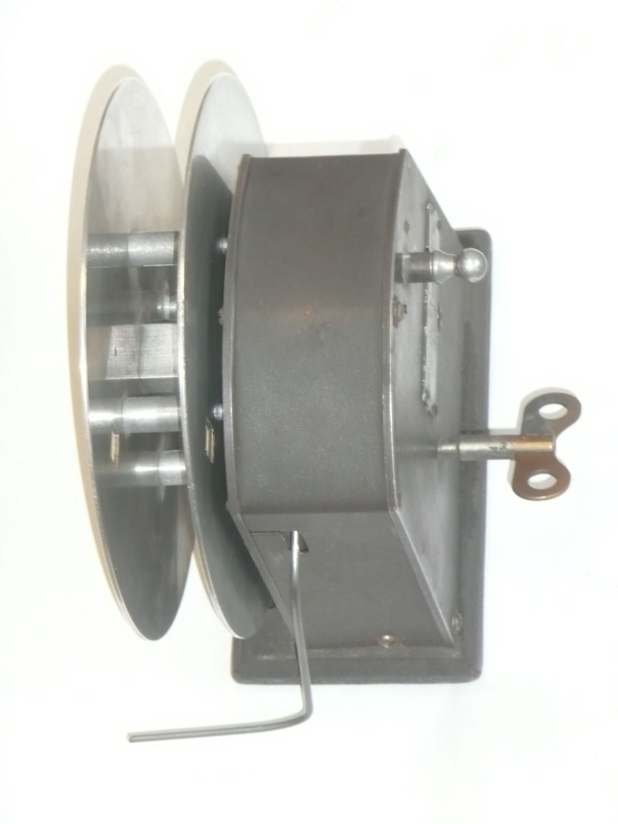
Music wire is both hard to bend and hard to cut, as it is tempered spring steel. We made the necessary cuts with an abrasive cut-off disk in a motor tool. In the case of the first cut, to the stub of the cut off control arm, the cut was inside the housing of the mechanism. Cutting steel with an abrasive disk, sparks fly, and among them are pieces of abrasive. We did not want to get abrasive in the mechanism, so we packed the area around our cut with paper towel before cutting.
After we made the cut, we assembled the case and then made two wide-radius bends in the wire, basing our bends on the drawing in "Teletypesetter Bulletin 57B, Parts for Tape Winders and on images from the web such as the Bunnel Winder in the Smithsonian, item 332416.
Only after making the bends did we cut off the excess length of our new
control arm.
Bug 64 and Bug 67: Continuing the work from Apr 7, we modified the diagnostic we'd written on Mar. 31 so that MSTART (location 00568) is 77008. This change makes our diagnostic run continuously over the final 64 words of memory. As of the end of our work on Mar 31, addresses of the form x2xx8 and x7xx8 were not working and we strongly suspected that the problem was in the board hand-numbered 9 in slot MD7. With this change to our diagnostic, it was constantly probing failed locations and not testing good ones.
With our diagnostic running, we began using our oscilloscope to measure the signals on the board in slot MD9. We had begun these measurements with poor results until we realized that we had serous scope grounding problems. During these poor measurements, our suspicion grew that Q5 was producing a corrupted signal. So, we hooked channel A of our scope (properly grounded) to the base of Q5 and used challel B to measure the signals leading there. Q5 is the inverting amplifier in a diode-transistor logic gate, so the natural places to test were the inputs to the diodes leading to Q5.
Whenever we tested D19, one of those diodes, the problem went away. Testing D18 and D20, two other inputs to Q5, had no effect. Our scope probes have spring-hook tips, and we were made each measurement by stopping the diagnostic, powering down the machine, hooking the probe in place, powering up the machine and restarting the diagnostic.
|
Re-soldering D19 fixed the problem. When we restored our memory diagnostic to make it test all of memory, addresses of the form x2xx8 still failed, but those of the form x7xx8 worked perfectly.
There was no guarantee that the remaining problem was on the same board, so we did a board swapping experiment:
| slot number | bad addresses | ||||
|---|---|---|---|---|---|
| MD6 | MD7 | MD8 | MD9 | ||
| board number | 8 | 9 | 6 | 7 | x2xx |
| 8 | 6 | 9 | 7 | x4xx | |
| 8 | 7 | 9 | 6 | x4xx | |
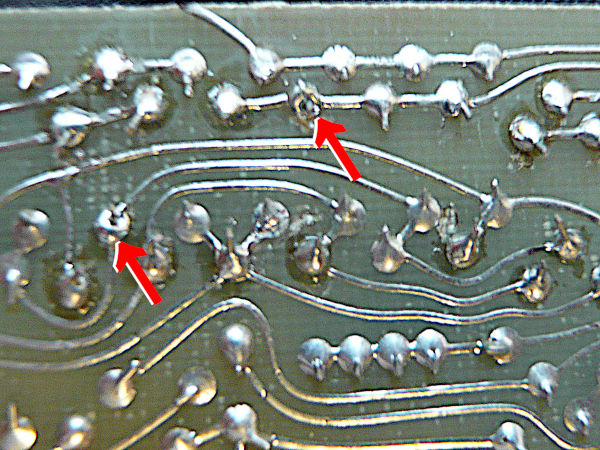
This test conclusively shows that our remaining problem is with the board numbered 9. We pulled this board again and began carefully measuiring the continuity of the solder joints to our replaced diodes. What we found was that the top solder joint to D49 was not connected. This solder joint looked good, but when we looked carefully at the photo shown above, we could see that the joint in the center left looked looked suspicious. Re-melting this joint fixed the problem.
With this job done, we ran our diagnostic and it ran continuously with no
error reports.
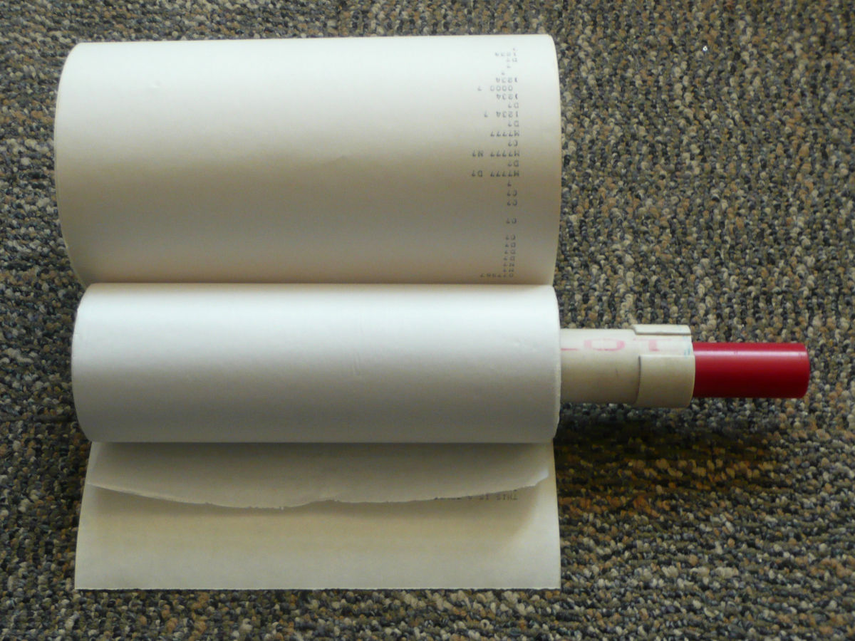
|
We used the same kind of 1" PVC drain pipe that
qrpbuilder.com
used, but instead of wrapping tape around the ends of pipe to make it fit the
paper roll, we used 1" long segments of the same pipe, slit and expanded to
fit as collars around the ends of our adapter and glued in place with PVC
solvent adhesive.
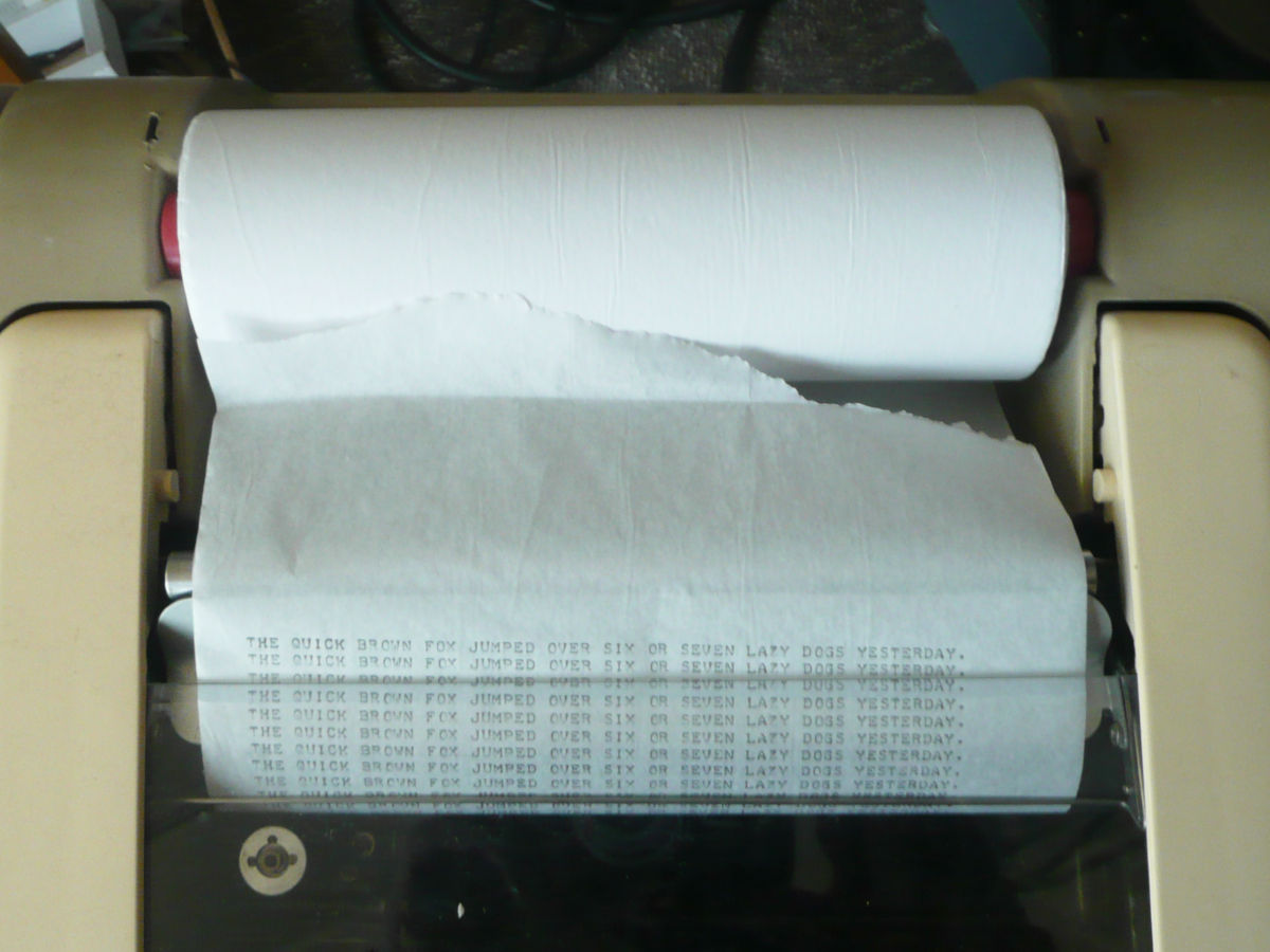
|
Bug 43: With the apparent resolution of our memory problems (Bug 64) on Apr 16, we noted that our memory diagnostic from Mar 31 had a problem: It only gives feedback about what it is doing when it finds an error. There is no way to monitor its successful execution. The code was still in memory, so we patched it.
Our original code would test the switch register after testing each memory location and halt at location 00478 if the switch register was zero. Continuing from this halt would continue the test. We replaced this halt with a jump to a block of code that put the address just tested into the accumulator before halting. Here is the patch, in assembly format:
           / Patch to memory tester
           *0047
00047 5057         JMP     PATCH   / replaces the halt
           RESUME,                 / return from patch here
           *0053
           MLOC,                   / address being tested
           *0056
00056 0063 MSTART, THEEND
00057 1053 PATCH,  TAD     MLOC    / AC = mloc -- AC was 0
00060 7402         HLT             / halt with mloc in AC
00061 7200         CLA             / -- AC back to 0
00062 5050         JMP     RESUME  / return from patch
           THEEND,
           $
We worked from paper in front of the console as we built the above patch, but here it is, integrated into the original code with better comments:
           / Little memory tester, tests all but low page 0
           / tests each location with 4096 possible values
           / does not disturb existing memory contents
           / show bad addresses in MQ.
           / if SR==0, tests just one word then halts
           / displaying the address most recently tested
           / continue from halt picks up at next word
           *0020
00020 7200 START,  CLA             / forever do
00021 1056         TAD     MSTART
00022 3053         DCA     MLOC    /   mloc = mstart
00023 7421         MQL             /   MQ = 0
           NEXT,                   /   for most of memory -- AC == 0
00024 1453         TAD I   MLOC    /     -- save value for later
00025 3054         DCA     MSAVE   /     msave = *mloc
00026 3055         DCA     MVAL    /     mval = 0
           RETEST,                 /     for all values -- AC == 0
00027 1055         TAD     MVAL
00030 3453         DCA I   MLOC    /       *mloc = mval
00031 1453         TAD I   MLOC
00032 7041         CMA IAC
00033 1055         TAD     MVAL
00034 7450         SNA
00035 5041         JMP     OK      /       if *mloc != mval
00036 7200         CLA
00037 1053         TAD     MLOC
00040 7421         MQL             /         MQ = mloc -- show addr
           OK,                     /       endif -- AC == 0
00041 2055         ISZ     MVAL    /       mval++
00042 5027         JMP     RETEST  /     endloop
00043 1054         TAD     MSAVE   /     -- restore original value
00044 3453         DCA I   MLOC    /     *mloc = msave
00045 7404         OSR
00046 7650         SNA CLA
00047 7402         JMP     PATCH   /     if SR==0 go show mloc -- AC == 0
           RESUME,
00050 2053         ISZ     MLOC
00051 5024         JMP     NEXT    /   until end of memory -- AC == 0
00052 5020         JMP     START   / forever
00053 0000 MLOC,   .-.             / addr being tested
00054 0000 MSAVE,  .-.             / save value that was in *mloc
00055 0000 MVAL,   .-.             / value used for testing
00056 0063 MSTART, THEEND
	   PATCH,                  / -- AC == 0
00057 1053         TAD     MLOC
00060 7402         HLT             / halt with mloc in AC
00061 7200         CLA             / -- AC back to 0
00062 5050         JMP     RESUME  / return from patch
           THEEND,
           $
With this code in place, we ran a total of 3 test cycles through all of memory with no error reports.
Having done this, we loaded the RIM loader (the Read-In Mode loader) throught the front panel switches. We used the version of RIM shown in Table 8-3 on page 8-7 of the PDP-8 Maintenance Manual, F87, Digital Equipment Corp., 1966. RIM load tapes are inefficient but easy to load, with each 12-bit load value preceeded by a 12-bit address, and each 12-bit value represented as 2 consecutive characters punched on tape.
We then used RIM to load the BIN loader from the Teletype, using a DEC paper tape from early 1967. BIN accepts a more compact binary data representation, with addresses included for each assembly origin followed by arbitrarily long data blocks. 12-bit values are still recorded as 2 consecutive characters, but load times (and tape lengths) are almost halved compared to BIN tapes. We then used BIN to load a 1967 BIN tape of ODT (the Octal Debugging Tool). The tapes we used were marked as follows:
The high-memory version of BIN in address 70008. When we started ODT, it output a CR-LF to the Teletype, but we had difficulty getting it to do anything but output question marks in response to our input. It turns out that we were using the wrong manual.
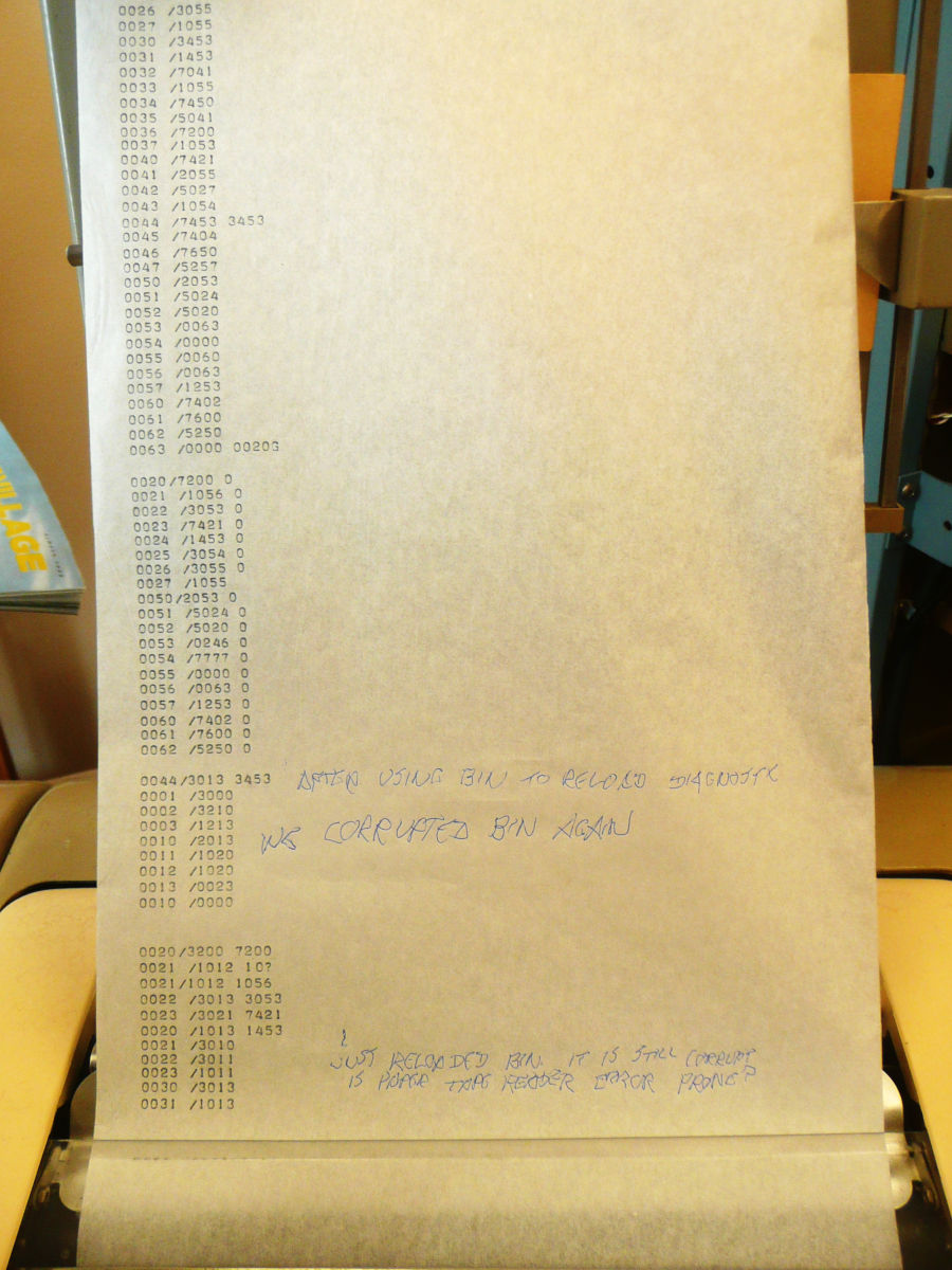
|
In the transcript shown, we only used three ODT commands, the forward slash, carriage return (CR), and linefeed (LF).
The first part of the listing shown here was produced by a sequence of linefeed commands stepping through and examining the memory diagnostic after using BIN to punch it to tape. Two words seemed to be misread (or mispunched), so we used ODT to correct them.
The middle part of the listing shows use of ODT to zero out part of our diagnostic. We then reloaded the diagnostic from paper tape and tried to examine it. At this point things went funny. The problematic part of our ODT session is transcribed below:
0044/3013 3453
0001 /3000
0002 /3210
0003 /1213
0010 /2013
0011 /1020
0013 /0023
0010 /0000
To produce the above, we typed 0044/ to examine location
00448. The value 30138 was wrong, so we typed
3453 followed by 7 linefeeds to examine the next 7 consecutive
locations. The addresses shown should have been consecutive, but instead,
the sequence is
00448,
00018,
00028,
00038,
00108,
00118,
00138 and
00108.
We do not understand what is wrong. Is there a CPU problem? Has the
Teletype paper-tape reader misread some of our BIN tapes?
Bug 43: We ended work on Apr 21 concluding that something was wrong but unsure what. One possibility is a problem in the CPU. The one large area of CPU behavior we have not explored carefully is autoincrement addressing. So, we wrote a little diagnostic:
           / diagnostic to test tad autoincrement addressing
           / display failures in MQ

           /TEST=  0010    / autoinc location from 0010 to 0017
           TEST=   0017    / (comment out one or the other)
           *0100
00100 7300         CLA CLL
00101 7421         MQL             / display = 0
00102 3017         DCA     TEST    / test = 0
00103 3123         DCA     TARGET  / target = 0
           LOOP,                   / for (;;) { -- assert AC == 0
00104 2123         ISZ     TARGET
00105 7000         NOP             /   target++
00106 1417         TAD I   TEST    /   test++
00107 7200         CLA             /   -- ignore the value loaded
00110 1017         TAD     TEST    /   -- see if test==target
00111 7041         CMA IAC
00112 1123         TAD     TARGET
00113 7450         SNA             /   if (test == target)
00114 5104         JMP     LOOP    /     continue -- assert AC == 0
00115 7200         CLA
00116 1123         TAD     TARGET
00117 7421         MQL             /   display = target
00120 1123         TAD     TARGET
00121 3017         DCA     TEST    /   test = target -- fix the error
00122 5104         JMP     LOOP    / } -- assert AC == 0
00123 0000 TARGET, .-.     / value we expect in TEST
We ran this diagnostic testing both the first and last autoincrement locations, addresses 00108 and 00178 and it ran continuously, auto-incrementing through all 4096 memory addresses as it read them using the TAD instruction. We let the program run for over a minute before we stopped it.
We then set out to write a similar diagnostic that used DCA. The code
for that proved to be more difficult to write since we need to avoid damaging
the program itself and we need deal with autoincrment stores to the
autoincrement location itself. This is a fun programming problem that we did
not complete.
Bug 43: We ended work on Apr 23 knowing that some rare instruction was not working. Having ruled out autoincrement addressing, we noticed that all of our testing of shift instructions used one-place shifts. We looked at drawing RS-D-R210 PDP-8 Accumulator, which describes R210 board. This is a 1-bit wide slice of the accumulator and arithmetic-logic unit. On this board, the data path for the 1-bit and 2-bit shifts are different.
This led us to write a little diagnostic that compares the RTR (rotate 2 places right) instruction with 2 iterations of the RAR instruction (rotate 1 place right).
           / RTR diagnostic (doesn't check link bit)
           / bad bits of AC are indicated by the MQ display

           *200
           START,
00200 7200         CLA
00201 7421         MQL             / MQ = 0
           LOOP,                   / forever {
00202 2220         ISZ     VALUE   /   value++ -- all possible values
00203 7300         CLA CLL	   /   -- clear link before shifting
00204 1220         TAD     VALUE
00205 7012         RTR
00206 3221         DCA     TESTIT  /   testit = value >> 2
00207 7300         CLA CLL	   /   -- clear link before shifting
00210 1220         TAD     VALUE
00211 7010         RAR
00212 7010         RAR             /   AC = (value >> 1) >> 1
00213 7041         CMA IAC
00214 1221         TAD     TESTIT
00215 7440         SZA
00216 7421         MQL             /   if (testit != AC) MQ = testit - ac
00217 5202         JMP     LOOP
00220 0000 VALUE,  .-.
00221 0000 TESTIT, .-.
As indicated in the comments, this code only checks the 12 bits of the accumulator, it does not check that the RTR instruction leaves the correct value in the carry bit. In our original code, we forgot to set the link bit to a predetermined value before shifting. After we found that error, we ran the code and saw the following displayed on the MQ lights:
This indicates that we were unable to shift the correct value into bit 2 of the accumulator. DEC's drawing BS-D-8P Accumulator and Link shows that the R210 board in backplane slots PA9 and PB9 holds bit 2 of the accumulator, so we exchanged this board with its neighbor in slots PA10 and PB10 to see if this moved the problem. It did, our output was now
In more detail, note that the value shown is
(value >> 2) - ((value >> 1) >> 1)
Assuming that one-place shifts work, a value shuch as 001002 therefore means that a bit was loaded with a one when it should have been zero, which is to say, the reset input to one of the fliplfops in the accumulator did not work when it should, or the set input worked when it should not. A value such as 111002 would indicate the opposite.
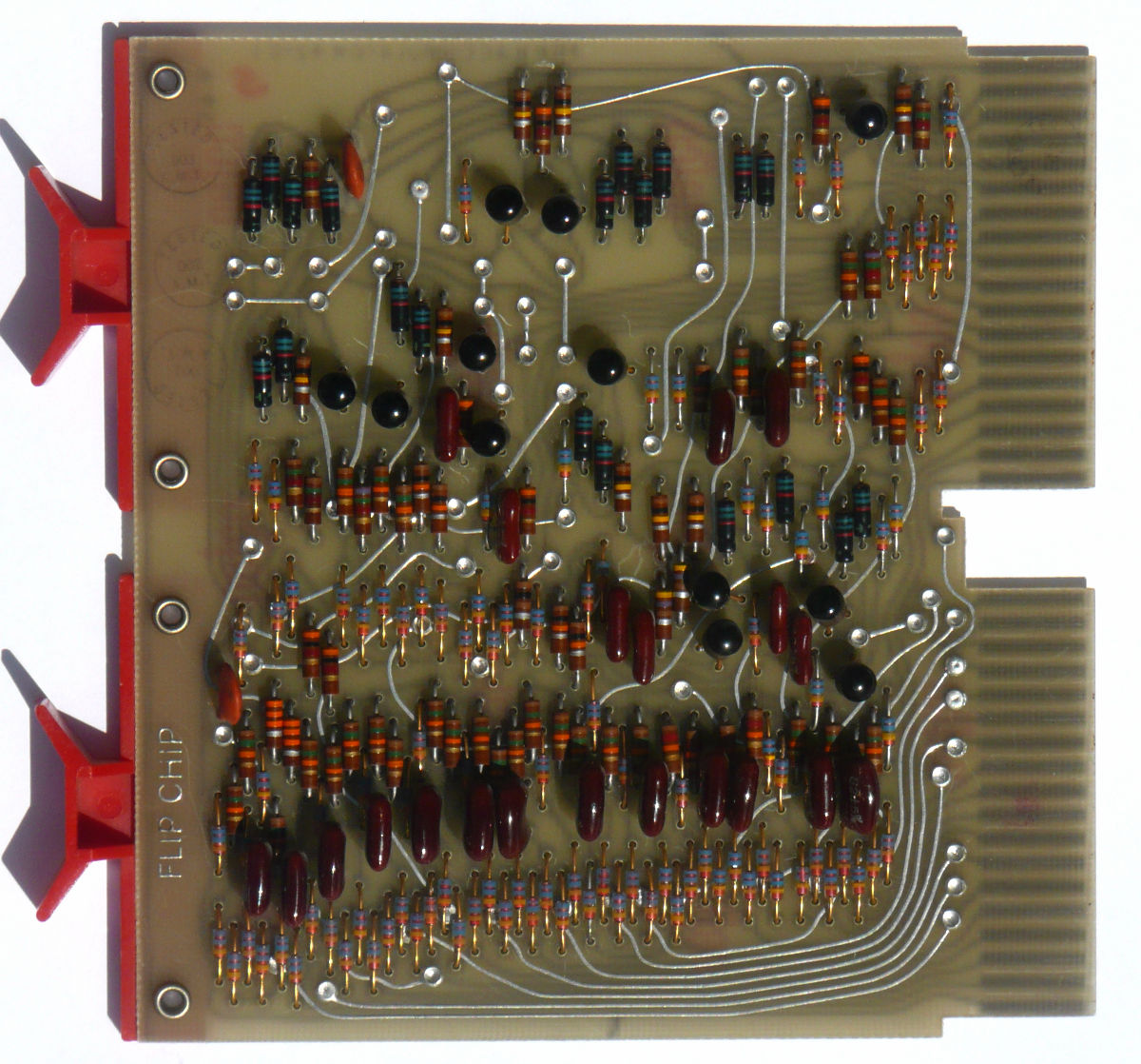
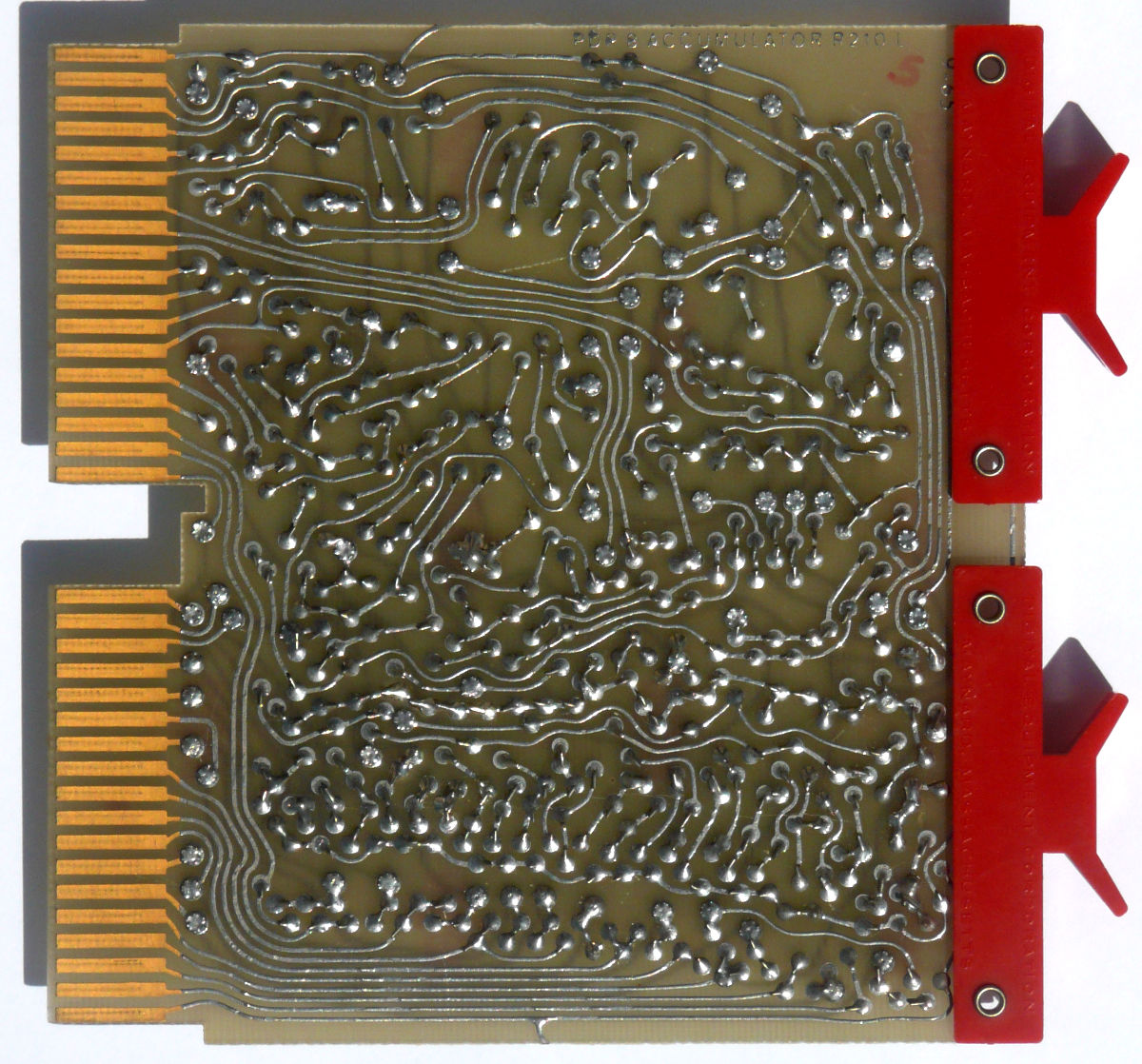
|
|
We spent some time searching the board with
an ohm meter and jeweler's loup and failed to find any problems.
This double-high board
has more that 120 diodes, 50 resistors, 20 capacitors and 10 transistors, and
some of the components are so tightly packed that it is difficult to probe
the component leads with an ohm meter.
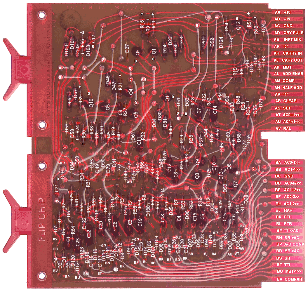
|
The parts of the CAD drawings that we could read made our work much simpler,
but we did find one error in that work. The parts shown in the CAD drawings
as R67 and R68 are diodes on our board, not resistors, and they are labeled
as D52 and D75 in DEC's schematic.
We began testing the problem R210 board with our RTR diagnostic from Apr. 28 running. We generally stopped the program and powered down the machine whenever we moved a scope probe from one point to another. Also, to verify that we were still looking at the correct circuit board, we swapped the R210 board in backplane slots PA10 and PB10 with the board in slots PA11 and PB11. Before the swap, the output was
After the swap, the output was
We used a Douglas Electronics clone of a W984 module extender to mount the problem R210 board in its backplane slot and connected channel A of our oscilloscope to the RTR input to this board. This input is pulsed each time the RTR instruction is executed. The most convenient place to clip a scope probe to measure this signal is the anode of D14, the diode that clamps this input to prevent it from going positive.
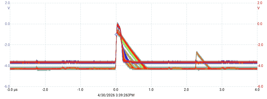
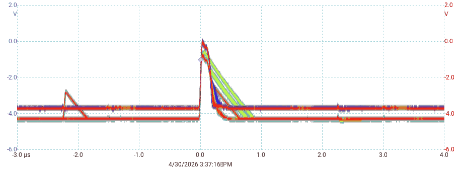
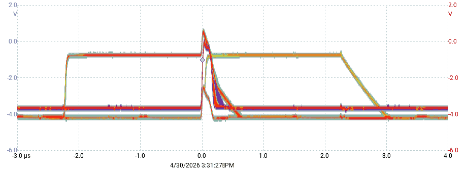
When the computer is running but not using RTR instructions, the RTR signal sits between -3.5V and 3.7V with scattered noise spikes that occasionally reach -3.3V or 3.9V. When we ran our dagnostic from Apr 28, each RTR instruction triggered a positive pulse with a peak between -0.3V and 0.1V, with a pulse width of just over 100ns at -1V. We left channel A showing this pulse for all of our oscilloscope measurements, and all of our measurements show the same 7μs time interval.
The RTR pulse is an input to 2 diode-capacitor-diode gates (DCD gates) that are used to multiplex the inputs to the accmulator. DCD gates are a unique feature of DEC's discrete-component flip-chip logic, covered by US Patent 3334249 applied for in 1965 and granted in 1967.
| |||
|
IT took us a moment to understand the additional peaks. These DCD gates
are used to set and reset the flipflop holding one bit of the accumulator.
There are similar gates for each input to the accumulator, and if one of the
other DCD gates clears the accumulator, that clear pulse will be coupled
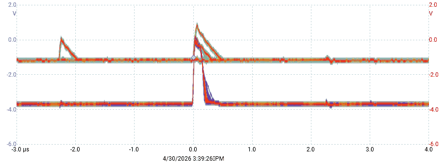
In our diagnostic, each RTR instruction is immediately preceeded
by a TAD instruction that will set each bit of the accumulator
half of the time.
The set pulse, if needed, occurs about 2.25μs before the RTR pulse.
Similarly, the following instruction is a DCA
that will clear the bit half of the time.
The clear pulse, if needed, occurs about 2.25μs after the RTR pulse.
| |||
|
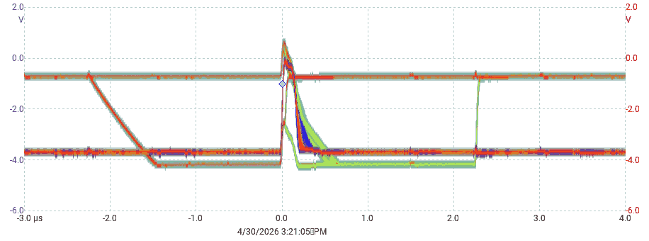
Prior to the preceeding TAD instruction, the data is 0. Then a 0 or a 1 is loaded. 2.25μs later, the RTR pulse is coupled through the capacitor in the DCD gate. If the signal was low, this produces a positive pulse up to about -2.5V. If the signal was high, a positive pulse up to about +0.7V occurs. This same activity occurs at all the flipflops in the accumulator, loading a new bit into all of them, so after this pulse, 50% of the time, signal will switch from high to low or low to high.
A close look at the central pulses measured on D17 and D109 shows nothing suspicious. The diode-capacitor part of these two gates seems to be working correctly. When we were taking all of our other measurements, our diagnostic held the MQ register constant at
Whenever we connected a scope probe to D109, however, the diagnostic output changed to
Something is wrong. D109 is on the set side of the flipflop, so the output with no probe indicates that the RTR pulse always sets, but with the slight load of the scope probe, the RTR pulse never sets.
We also checked final diodes in the DCD gates, D25 and D108.
These multiplex the outputs of the DCD gates onto the set and clear inputs
of the flipflop through two more diodes, D52 (clear) and D75 (set). The
latter diodes were in sufficiently uncluttered locations that we could
attach our scope probes to them, while D25 and D108 were in more crowded
parts of the board.
| |||
|
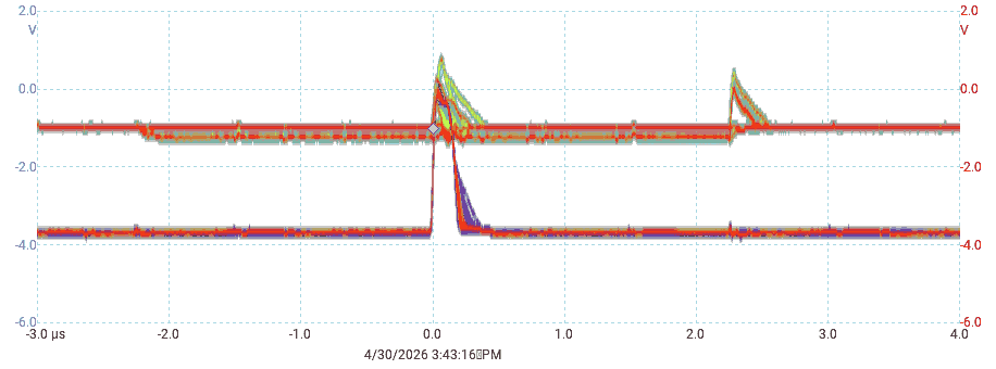
The scope trace for D75 shows the set pulse from the TAD instruction, and the trace for D52 shows the clear pulse from the DCA instruction. These are as expected, but there is an obvious difference between the measurements for D52 and D75: The measurement for D52 shwos two different voltages – a double line, sometimes resting at 1V, but at other times, dropping down to 0.75V. Nothing similar happens at D75.
We are puzzled by these results. If there is a problem on the general set
and reset lines for the flipflop, why does anything work. Specifically,
why does RAR work but not RTR, since both use DCD gates
to multiplex onto the same set and reset lines. We need to do more work.
Bug 86: We found a spare R210 board with a bit of masking tape residue on it that preserved, in ballpoint pen, the words "FOX SPARE." (Recall that this machine was originally purchased to support research directed by Stephen Fox.) We tried this board with our RTR diagnostic from Apr 28 and it did not work.
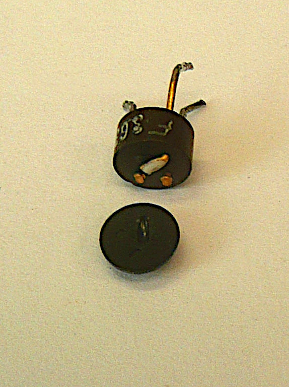
Testing the diodes on the board with an ohm meter, all appeared to be good, but continuing the tests with the transistors, we immediately found that Q7 and Q8, the two transistors that make up the flipflop holding one bit of the accumulator, were not the same. Our analog ohm meter showed 400Ω when measuring both junctions of Q8 in the forward direction, but the needle barely moved when doing the same measurements on Q7.
|
With the transistor removed from its crowded context, we also noted that it was a 2N3637 transistor, while DEC's drawing RS-D-R210 PDP-8 Accumulator indicates a DEC3639 transistor, where the spare parts list in the maintenance manual mentions the 2N3639. We doubt that these transistors are sufficiently different to make any difference, and we replaced it with a 3639.
Bug 43: Amazingly, this fix seems to work! We used the RIM loader to load the BIN loader, and used that to load the ODT debugger. Running ODT from the Teletype, we successfully examined several of the programs we had in memory, and we used ODT to patchy our RTR diagnostic to test the RTL instruction and then launched that diagnostic from ODT.
Our success ended there. When we tried to punch out a paper-tape of our
memory diagnostic, and then read it back in, it did not work. It appears that
we corrupted the contents of memory during some of our switch fumbling.
Also note that we did not complete repair of the original R210 board.
Bug 86: Give that we have both a good R210 board and a defective board, we decided to compare the two, repeating measurements we made on Apr. 30 with a bit more care. As then, we used the RTR diagnostic we originally used on Apr. 28, and triggering the scope on the leading edge of the RTR pulse.
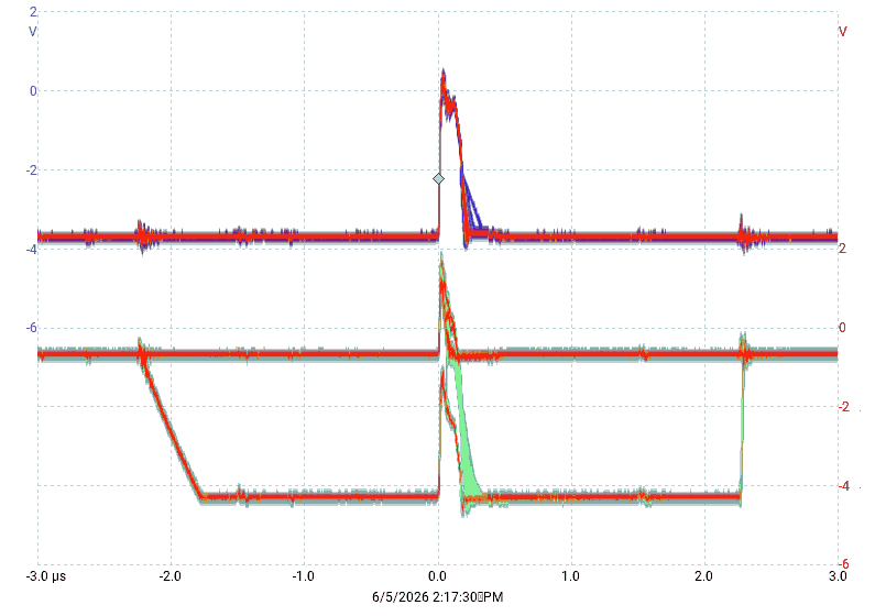
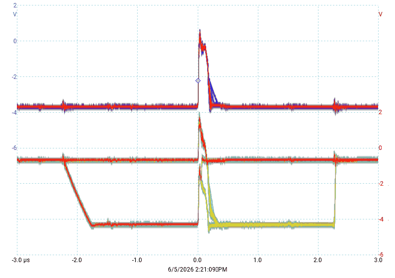
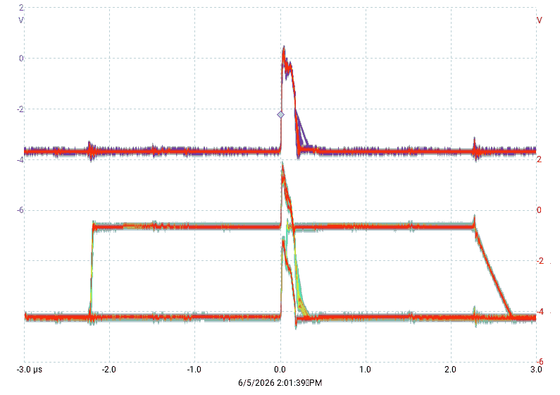
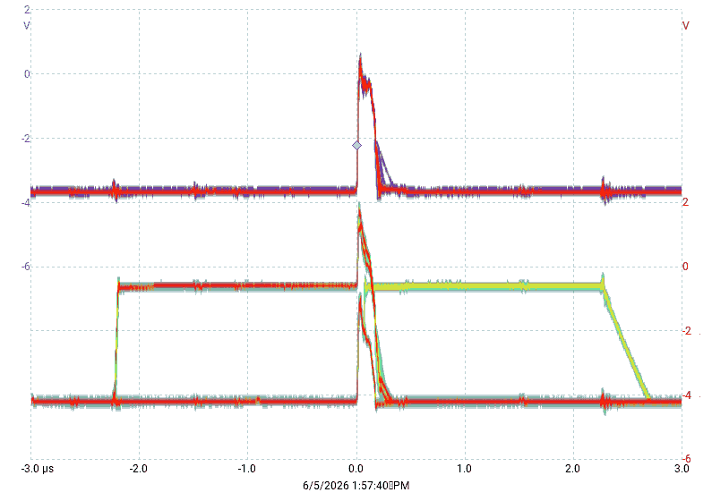
Aside from presenting side-by-side measurements of the two boards, the biggest change we made was to use the DC offset feature of our scope to move the RTR pulse uniformly up in every measurement so it does not overlap the signal we are looking at. The part numbers used in the following are all documented in the schematic for the R210 board, drawing RS-D-R210 PDP-8 Accumulator.
We began by looking at the internal nodes of the diode-capacitor-diode gates used to and the RTR pulse with the appropriate data on the set and reset sides of one bit of the accumulator.
|
| |
| Bad board | Good board |
|---|
Note that there is no discernable difference between the good and bad board
at this node.
|
| |
| Bad board | Good board |
|---|
Again, there is no discernable difference between the good and bad board at this node.
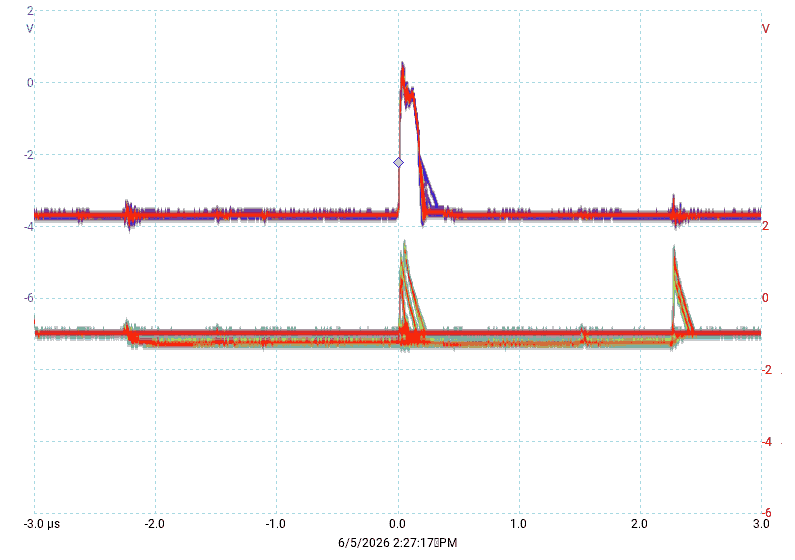
Our next focus was on the coupling of the diode-capacitor-diode gate outputs
to the set and reset inputs to the flipflop. Numerous DCD gates are
connected in a wired-or configuration to each flipflop input. Recall that
a DCD gate is a type of and gate, and the and-or cascade used
here forms a multiplexor to bring data from many potential sources into
the flipflop.
|
| |
| Bad board | Good board |
|---|
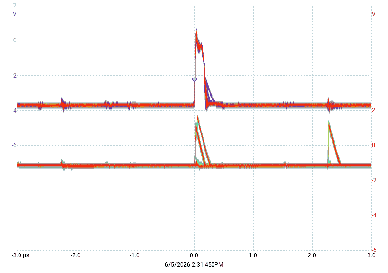
The circuit traces for this point show a distinct difference between the good
board and the bad one. On the good board, the idle voltage on the anode of
D52 is about -1.2V, while on the bad board, the idle voltage depends on the
value stored in the flipflop, sitting near -0.9V when the flipflop holds zero
and about -1.2V when it holds one. Something is definitely wrong here.
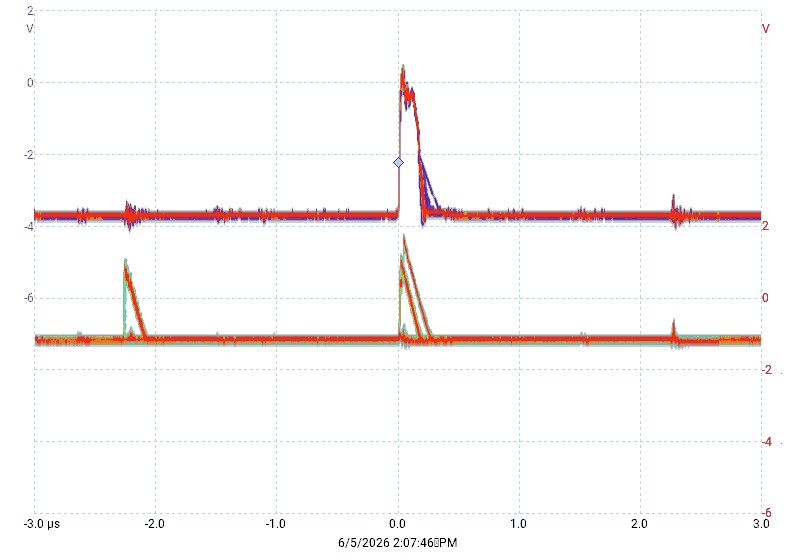
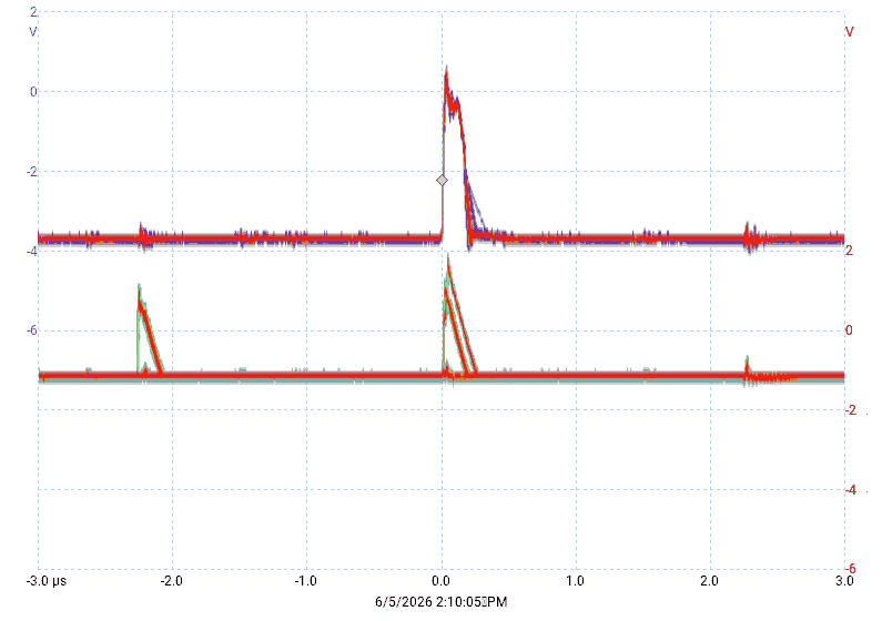
|
| |
| Bad board | Good board |
|---|
On the set side of the flipflop, the good and bad board behave identically,
with this node idling at about -0.12V except when some DCD gate delivers a
set pulse.
These measurements lead us to ask, what holds the idle voltage on the set
and reset wired-or lines? The schematic diagram
RS-D-R210 PDP-8 Accumulator
is very cluttered. Eventually, we found that the anode of D52 is
pulled up to ground through a pair of forward biased diodes, D51 and D50, with
the bias current flowing through R25 to -15V.
Similarly, the anode of D75 is pulled up to ground by D82 and D83 biased
through R41.
Nothing in the circuit should ever be able to pull either wired-or
node abouve the -1.2V value set by two forward-biased diodes in series.
Bug 86: Continuing the work from June 5, we hunted for differences between the R210 board labeled "FOX SPARE" and the defective board. Part names in the following discussion are given in the schematic drawing RS-D-R210 PDP-8 Accumulator, and the work we did on Apr 30 gives the physical part locations on the circuit board.
The first difference we found involved R25 and R41. These adjacent 33KΩ resistors both measured as 33KΩ on the good board in one direction, and 10KΩ in the opposite direction. The lower measurement is due to alternate current paths through diodes and other resistors.
The schematic shows that these two resistors pull the wired-or nodes on the set and reset sides of the flipflop down toward the -15V supply rail. On the circuit board, they are adjacent, about 1/3 of the way down the lower handle at the left side of the physical location map, and 4 or 5 components in from the handle.
On the bad board, R41 was the same, but R25 was 22KΩ. Our initial hypothesis was that R25 might be bad. To test this, we unsoldered one end each of both R25 and R41 so that we could measure their resistance without worrying about their circuit context. With this done, they both measured 36KΩ, which is close enough to their nominal value that we can rule out that hypothesis.
With R25 and R41 unsoldered, we measured the resistance from the wired-or nodes to the -15V rail. Because of the diodes in the current paths, we get two different values for each measurement. On the node that had been connected to R25, we got 40KΩ and 10KΩ. On the node that had been connected to R41, we got 140KΩ and 10KΩ. Because of the symmetry of the set and reset nodes to the flipflop, we expected these to be substantially the same.
The reset node is connectee to the -15V rail through D6, D11, D16, D25, D30, D38 and D50. These diodes are somewhat scattered on the board, but most of them are mixed in with resistors and capacitors in a row of components between the center of the lower handle on the board and the center of the lower card-edge connector. Many of these diodes are hard to probe because adjacent capacitors block easy access from the top of the board.
We checked all of these diodes using the times-10 scale on our ohm meter and found that most of them measured 200Ω in the forward direction and infinite in the reverse direction. The exception was D30, which measured 100Ω in the forward direction and 20KΩ in the reverse direction. This diode about 9 components in from the center of the lower card-edge connector. When we replaced it and soldered the resistors back in place, the board worked!
Going back to the RS-D-R210 PDP-8 Accumulator schematic, we note that D30 is part of the diode-capacitor-diode gate triggered by the RAR pulse, not the RTR pulse we had been focusing on. Our dignostic was comparing the RTR instruction with two repetitions of the RAR instruction, and we had assumed that it was RTR that was bad. We may have been wrong.
Why did we miss D30 in our sweep through the CPU boards looking for bad diodes? The answer may be simple: It was easy to examine all of the diodes in the long row of diodes along the bottom edge of the board. Those diodes stand out. Diodes elsewhere on the board are easy to miss because they are mixed in among resistors and capacitors.
Of course, it is also possible that this diode failed after our sweep through all of the diodes and after we ran our early tests of the RAR and RAL shift instructions. We will never know.