
The University of Iowa's DEC PDP-8Restoration Log
Part of
the UI-8 pages
|
The University of Iowa's DEC PDP-8Restoration Log
Part of
the UI-8 pages
|
This is a chronological log of the progress restoring the University of Iowa's PDP-8 computer. Entries are added at the end as work progresses. Click on any thumbnail image to see full-sized image.
|
|
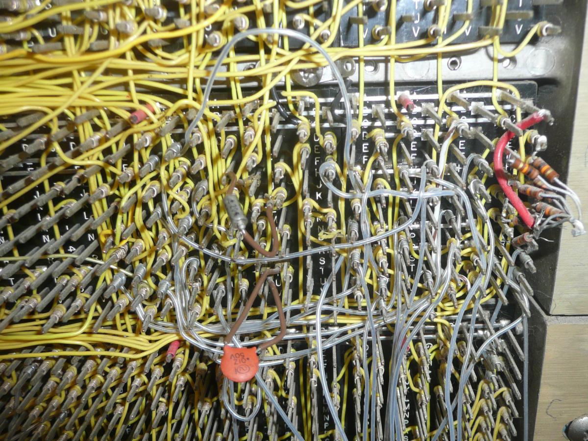
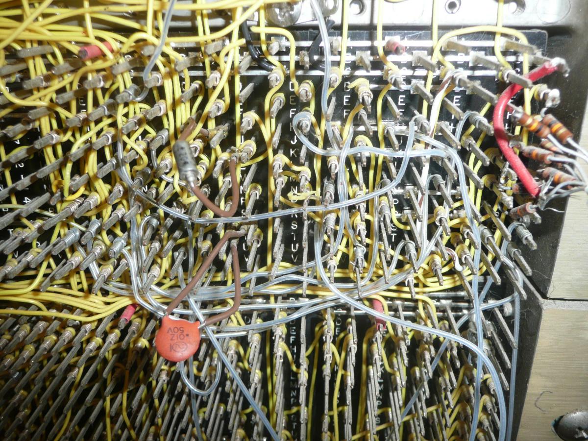
| Backplane rows B and D | |
|---|---|
| |
| Backplane wiring, as found | |
Several details are omitted here, notably, there were 7 wires from the data
inputs to the
R203 flipflops
in backplane slots B29 through B31 to an unpopulated backplane slot, D29.
These were all wires added by the Psychology department, and on careful
tracing their function, they all carried raw data from the tape reader.
Our best hypothesis is that these wires part of an unfinished project.
|
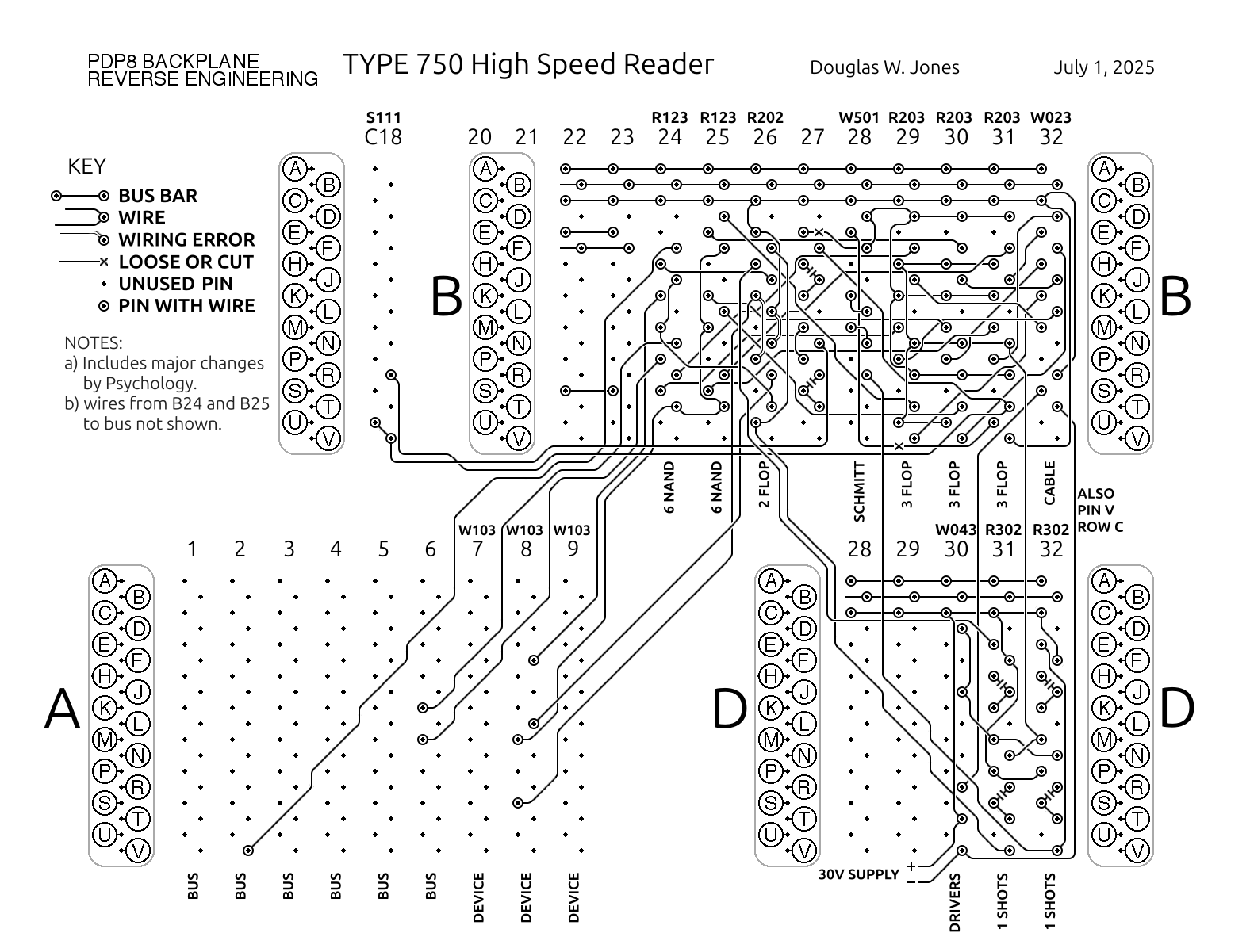
| Type 750 controller, as found |
|---|
The thing that was most apparent in reverse engineering this interface is that
it contains a number of features typical of shotgun debugging. The control
system is close to twice as complex as required for the Tally reader, and some
of the changes make this interface unnecessarily incompatible with the
documentation for the interface in the
PDP-8 Users Handbook
(Digital Equipment Corporation, 1966).
|
|
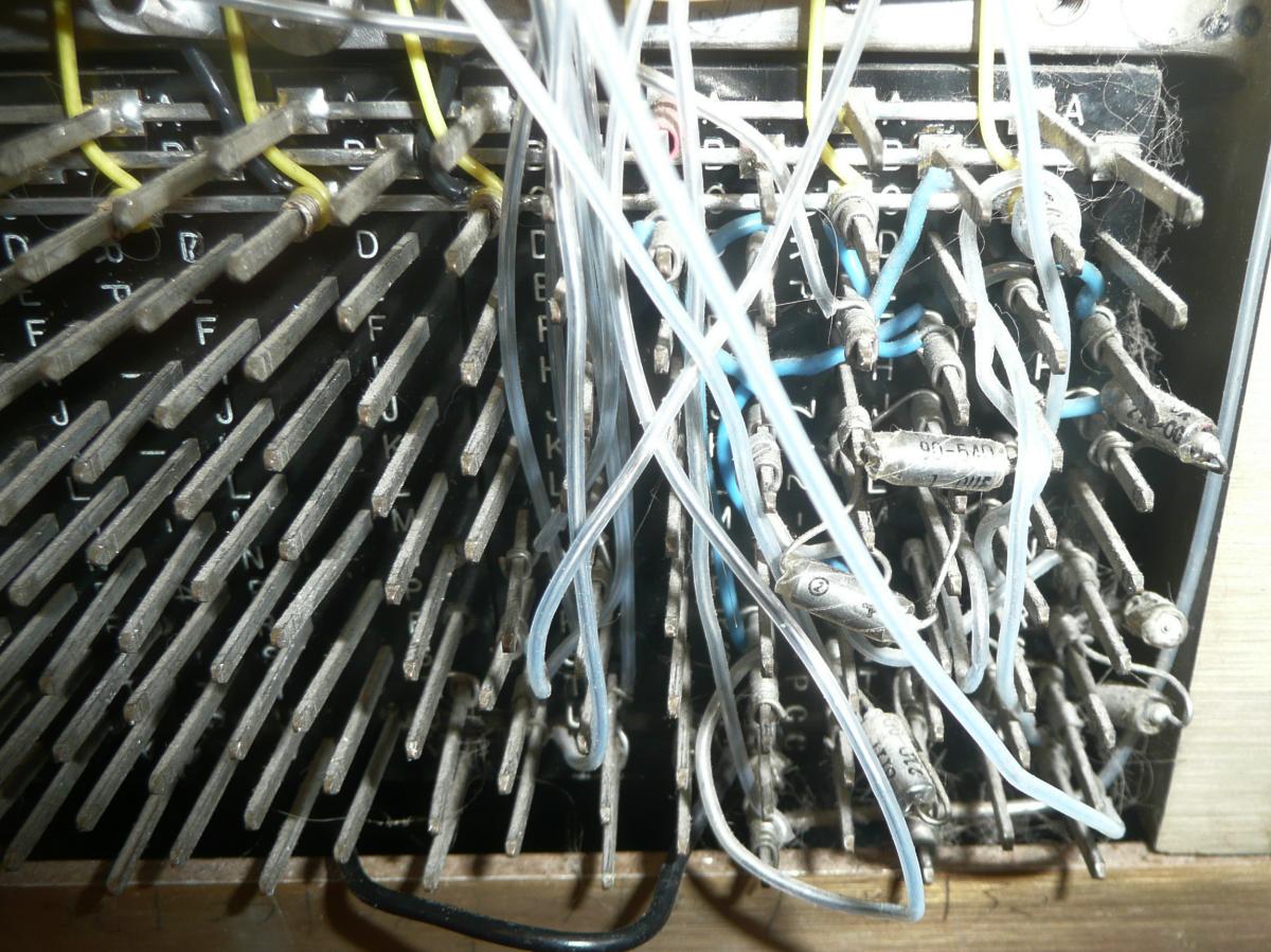
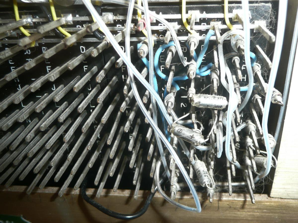
| Rows B and D cleaned up | |
|---|---|
DEC's backplane wire-wrap pins in the pre-TTL era were designed for 22 or
24 AWG wire using Kynar (polyvinylidene fluoride) insulation. Some of the
wire we removed had plain vinyl insulation, which is too soft for use among
the sharp corners of wire-wrap pins, and some was 28 or 30 AWG (we did not
measure it, but it was definitely too fine.) The blue wires visible in the
photo of row D above are examples of this problem that remain in place, for now.
|
|
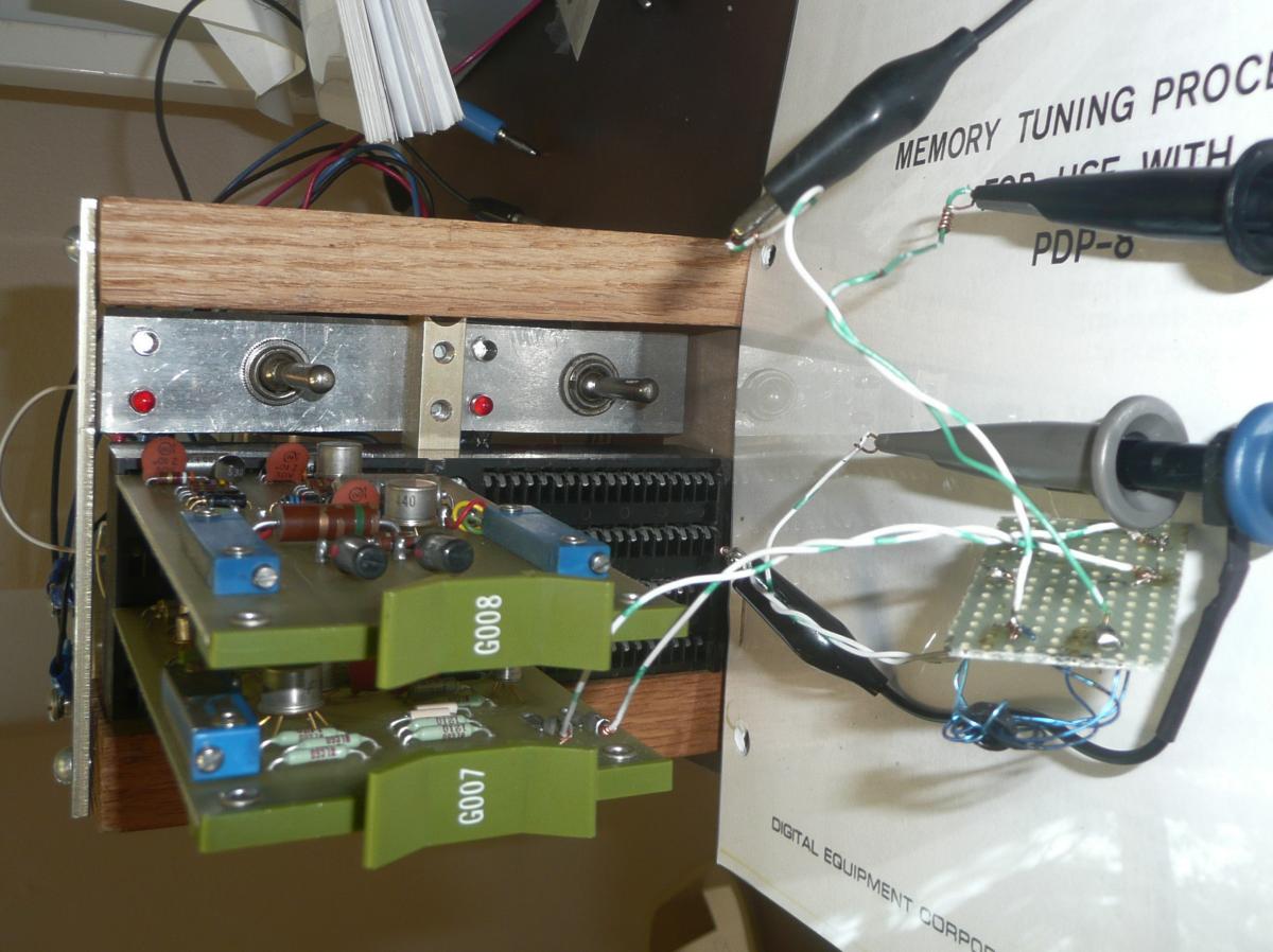
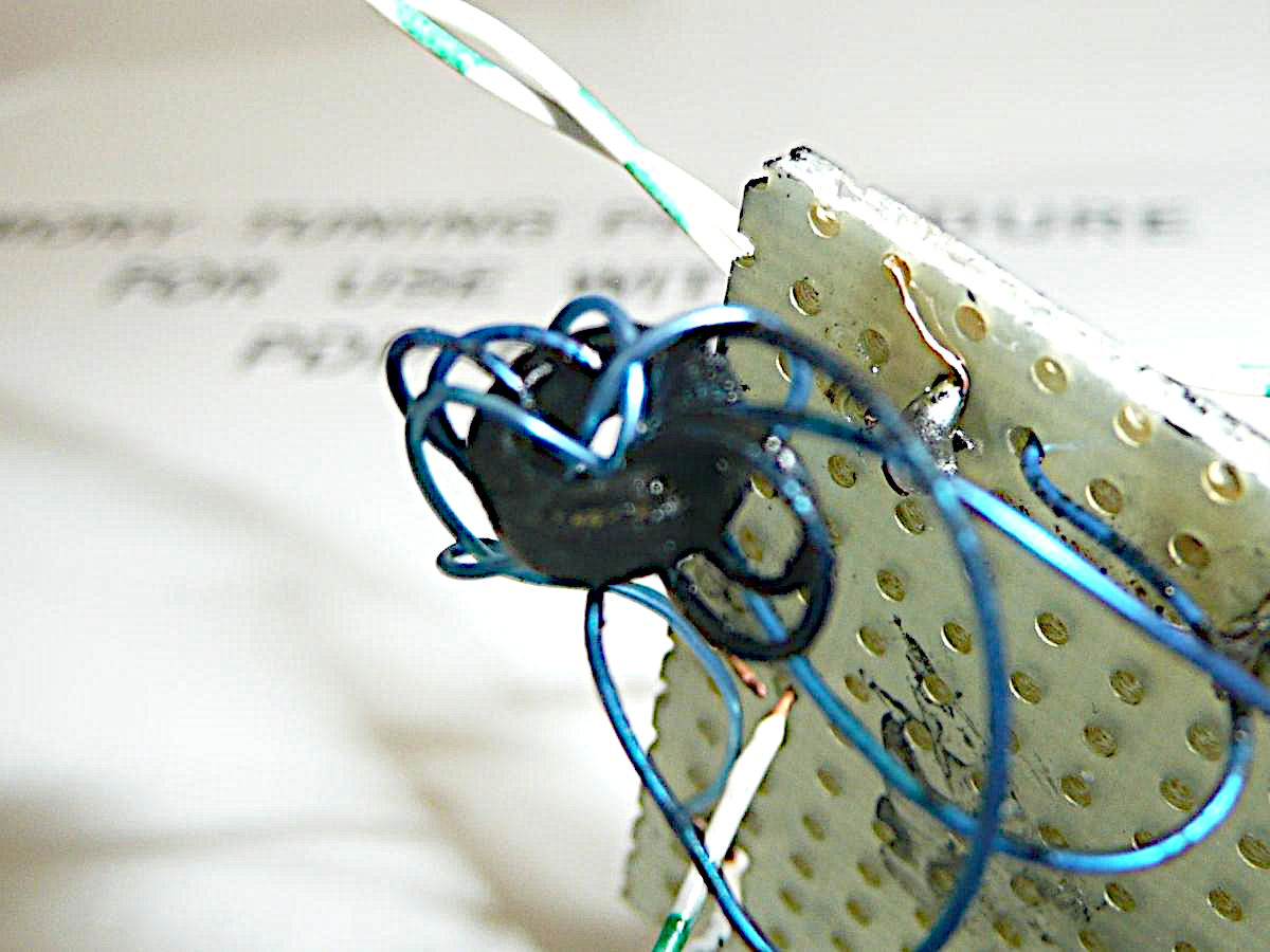
| The improved test rig | |
|---|---|
We broke the first small core we tried to use, ferrite is quite
brittle. To protect our second attempt, we mounted the core on a small circuit
board to isolate stresses on the windings from stresses imposed by test leads
and handling. Our core had with 3 identical 3-turn windings made of
30-gauge wire-wrap wire. One wining connected to the signal generator, one
to the input of the G007 board, and the final winding was used as a scope
input to monitor the input to the G007 without perturbing it. Driving the
core with a square wave produced nice spikes for testing the sense amplifier.
|
| Pins E & F of problem board. |
|---|
|
| Pins E & F of good board. |
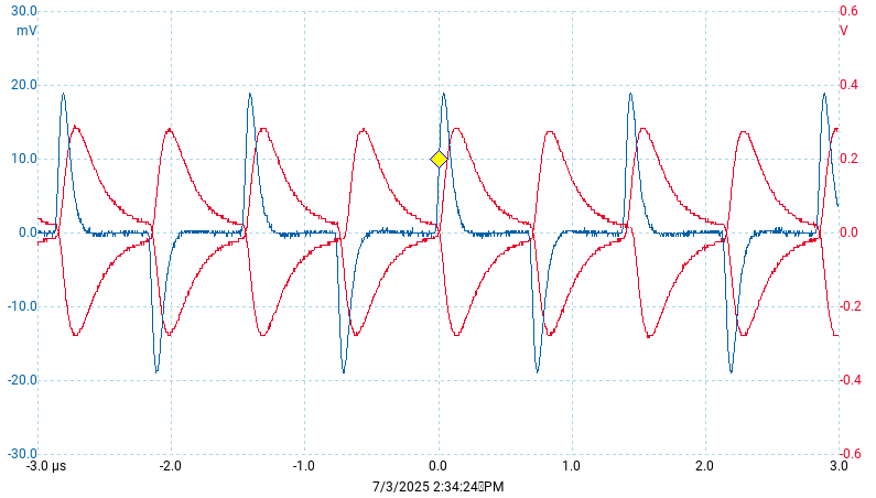
With our test rig producing clean 20mV spikes as input, the collectors of Q5 produce complementary and somewhat stretched spikes with an amplitude close to 0.25V. At first glance, it is very difficult to see any difference between the good board and the problem board. Note that the complementary outputs were recorded separately and then combined here. Small horizontal differences between the two red traces are the result of jitter in the signal generator output and not evidence of amplifier problems.
A closer look shows that the outputs of the good board are just shy of 0.25V,
while th outputs of the problem board are closer to 0.24V. A second detail
we noticed only on close inspetion was that the differential
amplifiers are not perfectly balanced on both boards. We did our best to
balance all of the amplifiers by adjusting
the trimmer potentiometer R4 to minimize the DC voltage between pins E and F,
as measured with an analog volt meter. The slight imbalance remaining shows up
as a slightly different peak amplitudes for the positive and negative spikes.
|
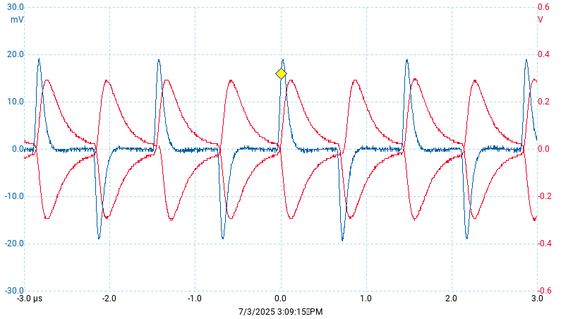
| Pin J of problem board. |
|---|
|
| Pin J of good board. |
The scope traces to the right show how the output of the slicer (shown in red) depends on the amplitude of the input pulses (shown in blue). We ramped the input pulse amplitude up from 30mV to 50mV. Note how, on the good sense amplifier, output pulses start to appear as the input amplitude rises from 30mV to 34mV, while on the problem board, output pulses only appear when the input amplitude rises from 38mV to 42mV. We used AC coupling for these measurements.
According to the writeup on the sense amplifiers on page 4-7 of the PDP-8 Maintenance Manual (Digital Equipment Corporation, 1966), the nominal amplitude of the input pulses to the sense amplifiers is 50mV.
Before we really thought this through, we replaced Q9 on the problem board.
While it is possible that insufficient gain in this transistor would lead to
problems here, it seems far more likely that what we are seeing is either
insufficient select current — leading to a low amplitude in the input to
the sense amplifier, or a slice voltage that is too high — leading to an
excessive threshold. The apparent big difference between the good sense
amplifier and the problem one can be explained by what we thought was
an insignificant difference between the two amplifier gains.
Bug 66: Having concluded, on July 3, that the most likely problem with our "bad" G007 sense amplifier board is simply that it has a lower gain than our "good" board, we set out to compare all 12 G007 boards. To help keep track of which board is which, we scratched an identifying letter on each board, from A to L, starting with the one we had considered bad. The following table relates board labels and bit numbers to backplane positions, as seen from the handle end of the board:
| ROW A | 30 | 29 | 28 | 27 | 26 | 25 |
|---|---|---|---|---|---|---|
| 10 | 8 | 6 | 4 | 2 | 0 | |
| B | C | D | A | E | F | |
| ROW B | 30 | 29 | 28 | 27 | 26 | 25 |
| 11 | 9 | 7 | 5 | 3 | 1 | |
| G | H | I | J | K | L | |
Note that, on the PDP-8, bit 0 is the most significant bit and bit 11 is the least significant bit. The bit numbers were taken from DEC drawing BS-D-BM-0-15 Sense Amps, Inhibit Drivers and Memory Control (page 10-51 of the 1966 Maintenance Manual).
With board A (the problem board) on the same test rig we used on July 3, we adjusted the slice voltage so that board A began to respond when inputs from the sense line had an amplitude of 34mV. In our July 3 tests, the good board (now labeled board J) had begun to respond at this voltage. (The slice voltage controls the threshold against which the differential amplifier output is compared, it is adjusted by changing the setting of the trimmer potentiometer R3 on the G008 Master Slice Control board; the schematic is immediately below that for the G007.)
We had adjusted the static balance of the differential amplifiers on all of the boards using the volt-meter techniqe recommended in the PDP-8 Memory Tuning Procedure (also available here) on page 9. We realized that our test rig offers a much more effective way to adjust the sense amplifier balance, so we adjusted the sense amplifier input to 50mV and then adjusted the sense amplifier balance so the output peaks on pin J were of equal height for both positive and negative input pulses. (Note that perfect balance was impossible because the balance adjustment, a 10Ω trimmer potentiometer (R4), changes the balance in discrete steps as the adjusting screw is turned.)
The following table shows the pulse height we measured on pin J for input 50mV input pulses on every board:
| Board | Pulse Height |
|---|---|
| A | -2.7V |
| B | -3.8V |
| C | -3.6V |
| D | -3.6V |
| E | -4.0V |
| F | -3.7V |
| G | -3.7V |
| H | -3.6V |
| I | -3.9V |
| J | -3.9V |
| K | -3.7V |
| L | -3.8V |
The data here makes it very clear that our problem board has an unusually low gain. We may need to replace on or both of Q2 and Q5, although it is also possible that the gain, although sub-par, will be tolerable after completing the memory tuning procedure.
Bug 64 and bug 66: On July 8 we speculated that our changed slice voltage might allow memory to work sufficiently reliably to allow us to try writing programs. So, we moved the G008 Master Slice Control (see schematic immediately below that of the G007) from our sense amplifier test rig back to slot B31 in the backplane and tried toggling things into memory.
Bug 43: It worked, so we tried writing a little program (all code here is shown in PAL-8 assember listing format):
00000 7001 L,      IAC             / increment AC
00001 5000         JMP     L       / iterate
Not a very exciting program, using just the IAC and JMP instructions, but it ran, with all the front panel lights for the accumulator AC blinking too fast to see, except the link bit L, a condition code bit that toggles with each carry out of AC. You could just see that L was flickering. We wanted to see what was happening, so we slowed the program down:
00000 7001 L,      IAC             / increment AC
00001 7000         NOP             / no opertion
00002 7000         NOP             / no opertion
00003 7000         NOP             / no opertion
00004 7000         NOP             / no opertion
00005 7000         NOP             / no opertion
00006 7000         NOP             / no opertion
00007 5000         JMP     L       / iterate
Adding NOP instructions slowed the program down enough that we could see that the top 3 bits of the accumulator were counting in binary.
With this success, we tried to make a program to run
chase lights
in the accumulator display:
Again this worked when we single stepped the code, but when we ran it,
it was too fast, nothing was visible on the front panel lights.
The
CLA, CLL
and
CML
opcodes all combine as a single microcoded instruction.
To slow it down, we tried adding a delay loop using the
ISZ
instruction:
This did not work. It hung in the delay loop, and when we single stepped the
code, we found that the carry was not propagating from bit 7 to bit 6 of the
delay loop counter X. Looking at the
CPU flow diagram, drawing
BS-D-8P-0-7 (page 10-55 of the 1966 Maintenance Manual),
we found that IAC and other addition functions on the accumulator
use a different incrementor than is used by the ISZ instruction.
The latter directly increments the memory data register, and according
to drawing
BS-D-8P-0-5 (page 10-35 of the Maintenance Manual),
carry propagation for that increment is done using a pair of
R181 boards.
We did not bother with reverse engineering, but simply pulled the board
from backplane slot PD19 (this
handles the carry from bit 7 to bit 6) and checked all the diodes. Two were
bad, so we replaced them and tried again.
With this fix, the program worked, but it was still too fast,
so we rewrote it as:
This program worked nicely, repeatedly moving a single one bit left through
the 13 bits [L,AC] slowly enough that you could follow it. We left it
running for several minutes, which is to say, many million instruction cycles.
Our attempts to write code that did load and store, or rather
TAD and DCA instructions
failed. We need to do more CPU debugging. We left
the chase light programm in memory before we turned the machine off because
it is good for quick demos.
Bug 43:
Continuing our work from
July 10,
we wrote more code. We were curious about taking input from the switch
register using
OSR.
At the same time, we experimented with writing code in
a higher
page
of memory, leaving our chase-light code from
July 10
in page 0:
This code worked. All it does is continuously display in the accumulator
whatever value is on the front-panel switches. This allowed us to quickly
verify that the data paths from all of the switches worked correctly. At the
same time, it demonstrates that the "current page" addressing mode works, at
least for
JMP
instructions.
We left that code in page 1 (which starts at 02008), and moved on
to page 2 (starting at 04008) for a test of load and store,
or rather
TAD and DCA instructions.
This program worked:
As written above, the front panel lights for the accumulator always show the
one more than the value in the switch register. Changing the final
JMP L to JMP M (52018) changes the
program's behavior to a simple binary counter.
From this experiment, we know that the DCA and IAC
instructions are referencing memory. Furthermore, they appear to be referencing
the current page, or at least, the chase-lights program we left in memory on
July 10
still worked correctly after running this program.
We left the following program in memory:
This program was somewhat fun becaue the value on the switch register
is the amount by which the counter is incremented for each iteration of the
outer loop, so by playing with the switch register while the program is
running, you can change the rate at which the higher bits of the counter blink.
We tried to load code in page 3 (starting at 06008 and had
difficulties. We tried to run larger programs and had difficulty. We tried
running programs with subroutines and had difficulty.
In some cases, these programs ran for a visible fraction of a second before
hanging, and when they hung, the code had been changed. This suggests that
there is something nondeterministic either in the call or return instructions
or dependent on memory addresses outside the first few addresses in a page.
We also noticed that setting the program counter to an odd address from the
switch register was difficult. It was easier to start with an even address and
then increment the program counter with the examine key.
00000 7320         CLA CLL CML     / initialize AC=0,L=0,L=~L
00001 7004 L,      RAL             / circular left shift [AC,L]
00007 5001         JMP     L       / iterate
00000 7320         CLA CLL CML     / initialize AC=0,L=0,L=~L
00001 2005 L,      ISZ     X       / increment X and skip if zero
00002 5001         JMP     L       / iterate delay loop
00003 7004         RAL             / circular left shift [L,AC]
00004 5001         JMP     L       / iterate
00005 0000 X,      .-.             / delay loop counter
00000 7320         CLA CLL CML     / AC=0,L=0,L=~L
00001 2011 L,      ISZ     X       / increment X and skip if zero
00002 5001         JMP     L       / iterate first delay loop
00003 2011 M,      ISZ     X       / increment X and skip if zero
00004 5003         JMP     M       / iterate second delay loop
00005 2011 N,      ISZ     X       / increment X and skip if zero
00006 5005         JMP     N       / iterate third delay loop
00007 7004         RAL             / circular left shift [L,AC]
00010 5001         JMP     L       / iterate
00011 0000 X,      .-.             / delay loop counter
Jul 15, 2025, More programming
00200 7604 L,      CLA OSR         / AC=0,AC|=SR (in sum, AC=SR)
00201 5200         JMP     L       / iterate
00400 7604 L,      CLA OSR         / AC=0,AC|=SR (in sum, AC=SR)
00401 3210 M,      DCA     X       / X=AC,AC=0
00402 7001         IAC             / AC+=1 (so AC=1)
00403 1210         TAD     X       / AC+=X (eventually increment X)
00404 2211 N,      ISZ     Y       / increment Y and skip if zero
00405 5204         JMP     N       / iterate delay loop
00406 5200         JMP     L       / iterate

00410 5200 X,      .-.             / value from SR or counter
00411 5200 Y,      .-.             / delay loop counter
00400 3210 L,      DCA     X       / X=AC,AC=0
00401 7604         CLA OSR         / AC=0,AC|=SR (in sum, AC=SR)
00402 1210         TAD     X       / AC+=X (eventually X=X+SR)
00403 2211 M,      ISZ     Y       / increment Y and skip if zero
00404 5203         JMP     M       / iterate delay loop
00405 5200         JMP     L       / iterate

00410 5200 X,      .-.             / counter visible on AC lights
00411 5200 Y,      .-.	           / delay loop counter
Jul 17, 2025, Test and replace some diodes
|
| The chase light test |
|---|
Bug 74: In 2017, we scanned all of the R210 and R211 boards (25 double-height boards in all) in the CPU for bad diodes and replaced several. See bug 49 and bug 61. We decided that it was time to scan all of the other boards on the CPU side of the machine for bad diodes, and we found 3 on the boards in row PA of the backplane. We accidentally mis-diagnosed 3 more as bad and replaced them as well.
Our mis-diagnoses were diodes where the reverse resistance, when measured with an ohm-meter on the ×10 scale, was less than infinite. Sometimes, this is due to the circuit context providing an alternate current path. Short of reverse engineering boards, the easy way to discover if this is the case is to have a spare board for comparison. Fortunately, we have a stock of spares, all of which we should eventually test.
Bug 43: The chase-light program we wrote on July 10 still worked, but we got a bit ambitious and decided to rewrite it to see if the MQ (multiplier-quotient) register in the extended arithmetic element works. This uses just two new instructions, MQL and MQA
00200 7201         CLA IAC         / AC=0,AC+=1
00201 7421         MQL             / MQ=AC,AC=0
00202 2214 L,      ISZ     X       / increment X and skip if zero
00203 5202         JMP     L       / iterate first delay loop
00204 2214 M,      ISZ     X       / increment X and skip if zero
00205 5204         JMP     M       / iterate second delay loop
00206 2214 N,      ISZ     X       / increment X and skip if zero
00207 5206         JMP     N       / iterate third delay loop
00210 7501         MQA             / AC=MQ
00211 7004         RAL             / circular left shift [AC,L]
00212 7421         MQL             / MQ=AC,AC=0
00213 5202         JMP     L       / iterate outer loop

00214 5200 X,      .-.             / delay loop counter
|
| Testing the MQ register |
|---|
Bug 64: We had to re-enter the program several times, as some bits of some instructions were repeatedly corrupted by attempts to run it. Once it ran, however, it kept running. We strongly suspect that we need to continue our memory tune up to fix this.
Bug 74:
We spent most of our time continuing the work we started on
July 17,
a systematic sweep through the diodes
on the processor side of the machine. While we are at that, we also began
systematically testing the diodes in our spare parts collection.
We found several bad diodes in both row PB of the CPU and in our spare parts
collection. Most of these were DEC's D664 diodes, but two were D662 diodes,
equivalent to 1N645, for which we have ordered a stock.
Bug 74: We completed our sweep of diode testing through the processor side of the machine and finished up by testing the diodes in the Teletype interface and bus drivers on the memory side, and through all the diodes on the memory select matrix boards. We also went through our unopened spare board collection (but not the spares in unopened intact original plastic bags).
| slot | type | diodes replaced | ||||
|---|---|---|---|---|---|---|
| PE33 | R602 | 1 D664 | ||||
| PE22 | S107 | 1 D664 | ||||
| PE20 | R111 | 1 D664 | 1 D662 | |||
| ME22 | R220 | 3 D664 | ||||
| MF14 | S202 | 1 D662 | ||||
The table to the right shows some of the diodes we replaced. In general, the D664 diodes (used in logic and to clamp input and output voltage swings) were more likely to fail than the D662 diodes DEC liked to use for their forward voltage drop.
Our diode tests were in circuit, using an analog ohm meter on the x10 scale. Good diodes (D662 and D664) had forward resistances that measured as 180Ω – 200Ω and reverse resistances that were either infinite or over 2000Ω for some diodes where the circuit context provided an alternate reverse current path.
Most diodes failures involved decreased resistance, measuring under 150Ω forward and under 1000Ω reverse, but a few failures tended toward an open circuit. For example, one D662 both in circuit and after unsoldering, measured about 400&Omega forward and infinite in reverse.
Bug 75:
During the diode scan, we found that the
W050 30ma indicator driver
in backplane slot MF23 is missing 3 of its 7 transistors.
The etch on this board identifies it as a W050B.
The
schematic
identifies these transistors as 4JX1C741 (equivalent to 2N527).
These are germanium transistors, and searching on line for them shows that
they are rare, apparently because designers of fuzz boxes for electric guitars
like to use them. The front panel has 82 of these transistors used as drivers
for the 82 lights there, and we suspect that these transistors were mined to
replace some on the front panel.
Examining drawing
BS-D-8M-0-11 Teletype Control
(page 10-46 of the 1966 Maintenance Manual), we found that only 2 channels on
this 7-channel board are in use, one to drive the serial data line, one to
drive the reader-run line. We verified this by checking that the
backplane wiring on slot MF23 does not connect to the other channels.
While the interface should work with this board partly populated, we found a
source for 4 used 2N527 transistors and ordered them.
Bug 76:
Aside from working on memory, next step will be to try to debug
the Teletype interface. When we plugged in the Teletype, it immediately began
to chatter. Something is wrong. We opened up the cover to investigate, and
found that the selector magnet was buzzing. This should not happen when the
machine is idle, but our initial attempt to diagnose the problem produced no
result. Reading drawing
FS-9 115VAC power distribution
in the Teletype model 33 drawing collection,
we did learn that the local-off-line switch on the Teletype leaves the power
on to the receiving circuitry and selector magnet in all positions.
Sep 22, 2025, Diagnose Teletype failure
|
| Voltage across power transistor. |
|---|
|
| Voltage across local loop supply. |
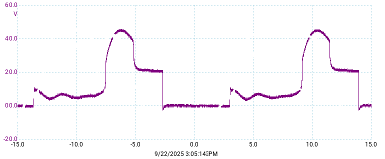
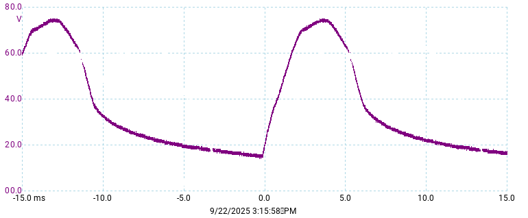
The transistors in the selector magnet driver are switched by the current in the data loop. When the Teletype is turned off or in local mode, this current is provided by the local loop supply. Drawing FS-1 Local Loop Current Supply in the Teletype model 33 drawing collection shows the local loop supply. This has a half-wave rectifier, so a failure in the filter capacitor, C1 in this drawing, would produce 60-cycle modulation of the local loop current. The second scope tract to the left shows the voltage across this filter capacitor.
Capacitor C1 has not shorted, but it's capacity is not high enough to sustain the loop current. It is a 250μFd 75V electrolytic capacitor, and our best hypothesis for the failure mode is that the electrolyte has been slowly drying out, reducing the capacity to a small fraction of what it should be. We ordered a replacement capacitor.
All of the scope traces shown here were taken in differential mode because
both the local loop supply and the selector magnet driver supply float
relative to ground.
Bug 76: We got a new 250μFd 75V electrolytic capacitor and put it into the Teletype's local loop supply. This immediately cured the problem with the Teletype chattering when plugged in but turned off.
Initially, there was something wrong when we switched it into local mode. Switching to local mode somehow opened the local loop. We cannot see how this could happen, and after a bit of fiddling, the problem seems to have fixed itself.
The old capacitor, to which we had added a bit of water, tested as better than it had been but not nearly as much capacity as the replacement, so we sealed the bung hole with black enamel paint and packed it awas as a spare part (perhaps more capacity will return, or perhaps we will eventually open the bottom of the can and stuff in modern replacements to create a cosmetically acceptable replacement part).
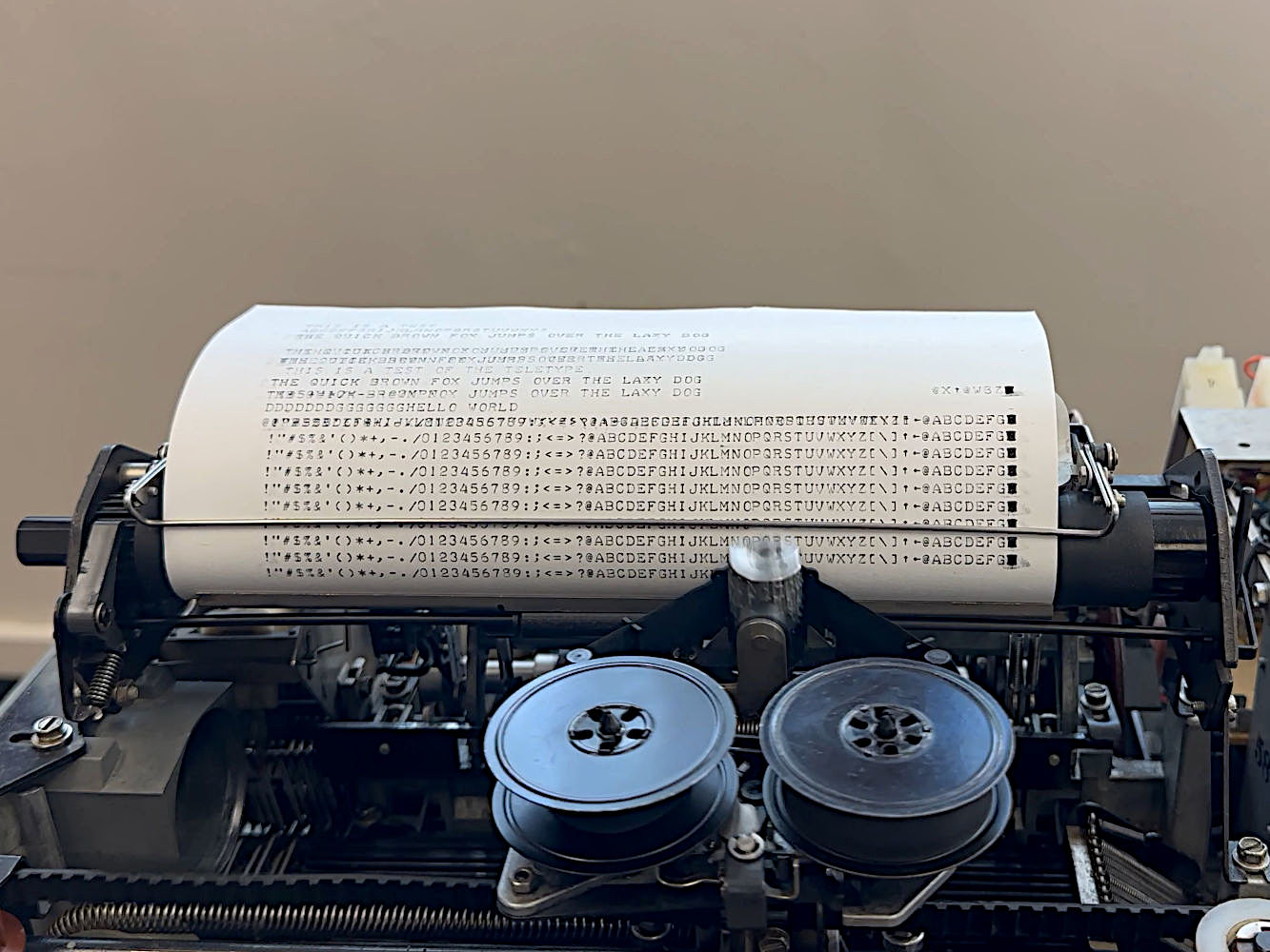
Bug 43: With the Teletype seeming to work, since we have completed our scan of all diodes in the PDP-8, we tried connecting everything and running a small program.The following program should have printed the entire character set over and over again including control characters and lower case (that the Teletype should fold into upper case):
06000 7200         CLA             / AC = 0
06001 6046 A,      TLS             / Loop top, send AC to TTY
06002 6041 B,      TSF             / skip if TTY done
06003 5202         JMP     B       / poll
06004 7001         IAC             / advance to next character
06005 5201         JMP     A       / iterate
This did not work, although resetting the computer did seem to send a null once in a while, a good sign that quite a bit is working. The program runs correctly on our emulated PDP-8/E, so we will need to do some work to diagnose the problem here.
Bug 74:
In the time that was left, we went back to scanning diodes in the
multifunction I/O device backplane
at the bottom of the I/O rack. We finished all of the
boards in rows A an B of this 4-row backplane, except for the double-high
device selector boards. We found bad diodes on 2 R203 boards, one in A18
and one in B16; each had one partially shorted D664 diode. We replaced these.
Bug 75: The 2N527 transistors we ordered on Sep 18, 2025 arrived (somewhat late because the first eBay supplier we ordered from lost them and refunded our money, leading us to seek an alternate source). We replaced the three that had been mined from the W050 board in backplane slot MF23, leaving two spares in our spare parts supply.
Bug 74: We finished scannig diodes in rows A and B of the multifunction I/O device backplane. Rows C and D remain to be scanned.
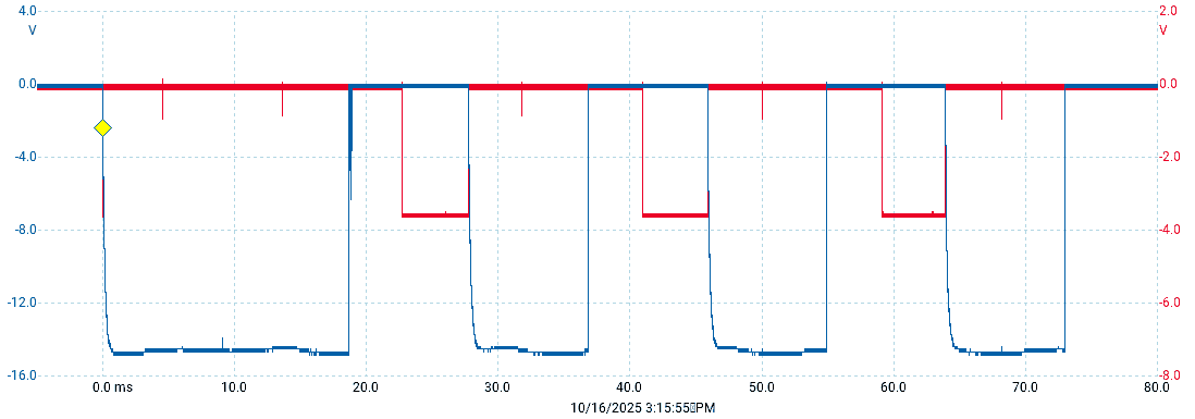
Bug 43 and created Bug 77: We verified that the test program we left in memory on Sep 29 was still in memory, and then it while using logic probes and an oscilloscope to trace signals in the teletype interface in rows ME and MF of the PDP-8. This is described in drawing BS-D-8P-0-5 (page 10-45 of the Maintenance Manual). We made the following observations:
ME15, an R405 crystal clock — pin D oscillates at 7.04KHz, as specified in the schematic.
MF16, MF15 and MF14, all R202 dual flipflops — the clock divider chain divides the clock by 64, producing the 110Hz signal needed for the 110 baud teletype on MF14 pin J.
MF18, an R603 triple pulse amplifier — pin D receives IOP 1 from the CPU every 5μs.
MF18 the same R603 – pins R and K receive IOP 2 and IOP 4 from the CPU just once each time the program is restarted.
Here is part of the code from Sep 29 with the comments changed to reflect Sep 29 the low-level meaning of the instructions:
06000 7200         CLA             / AC = 0
06001 6046 A,      TLS             / Loop top, send IOP 2 and IOP 4 to TTY
06002 6041 B,      TSF             / skip (send IOP 1 to TTY)
06003 5202         JMP     B       / poll
Our measurements show that the TSF instruction never skips! Why?
On closer inspection, we found brief negative spikes each time the flipflop
driving ME22 pin N was clocked, while pin U, the complement output remained
constant. This flipflop should reset when clocked,
and does not. We tried substituting our one spare R220; on that, pins N and U
were both stuck at 0V, suggesting a defective spare.
Bug 77: Continuing the work started on Oct 6, we pulled the R220 3-bit shift register board from backplane slot ME22 and rechecked the diodes. This board is very crowded compared to most of the boards in the machine, and the diodes are not uniformly oriented the same way on the board, making checking tricky. Working carefully, with a spare board for reference, we found 4 more bad diodes, all DEC's D664. We replaced them and tried the machine.
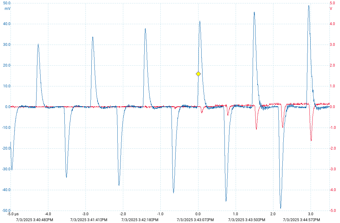
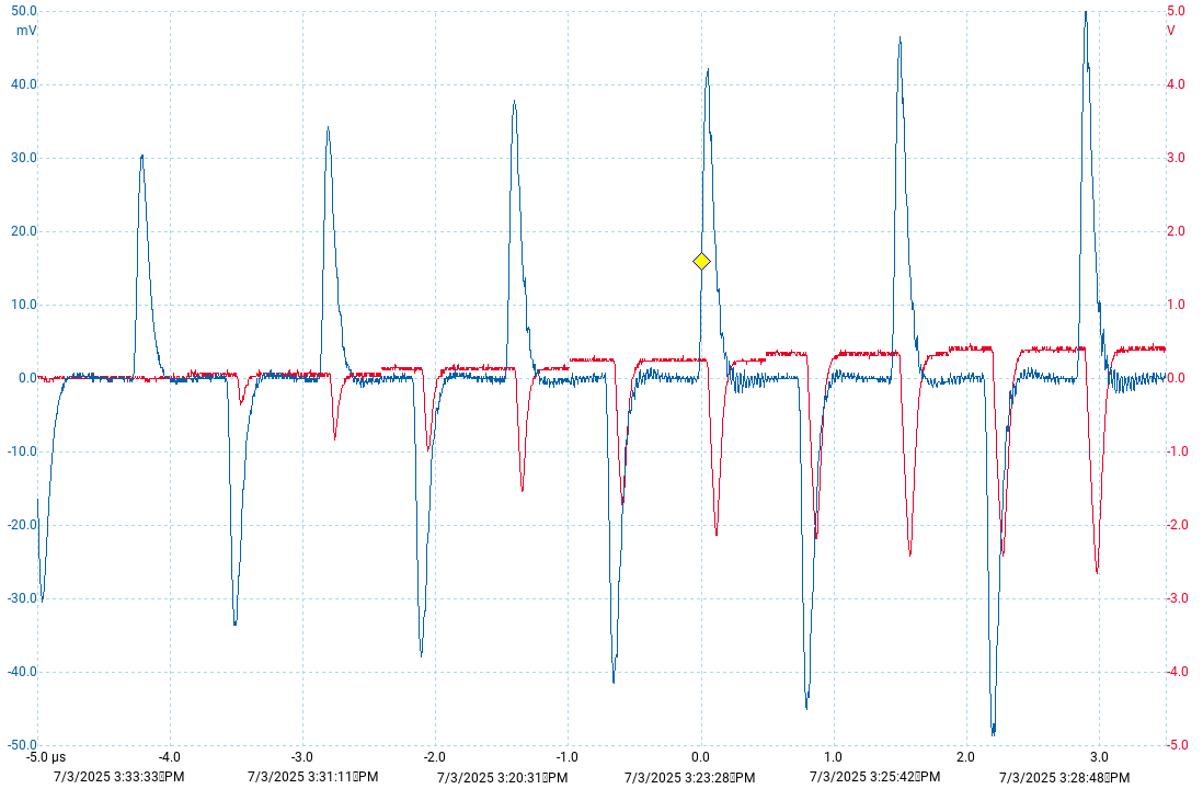
|
| First Teletype output |
|---|
Bug 62:
The photo is misleading. The linefeed mechanism worked only when characters
were typed from the keyboard. When driven at full speed from the data line,
line feeds were ignored -- but our test program outputs all 32 control
characters, giving ample time to reach in and manually advance the
paper.
| |
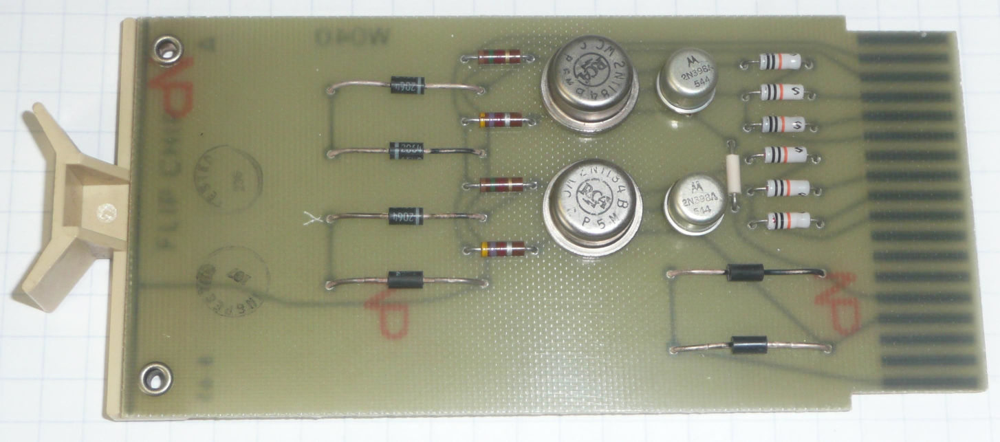
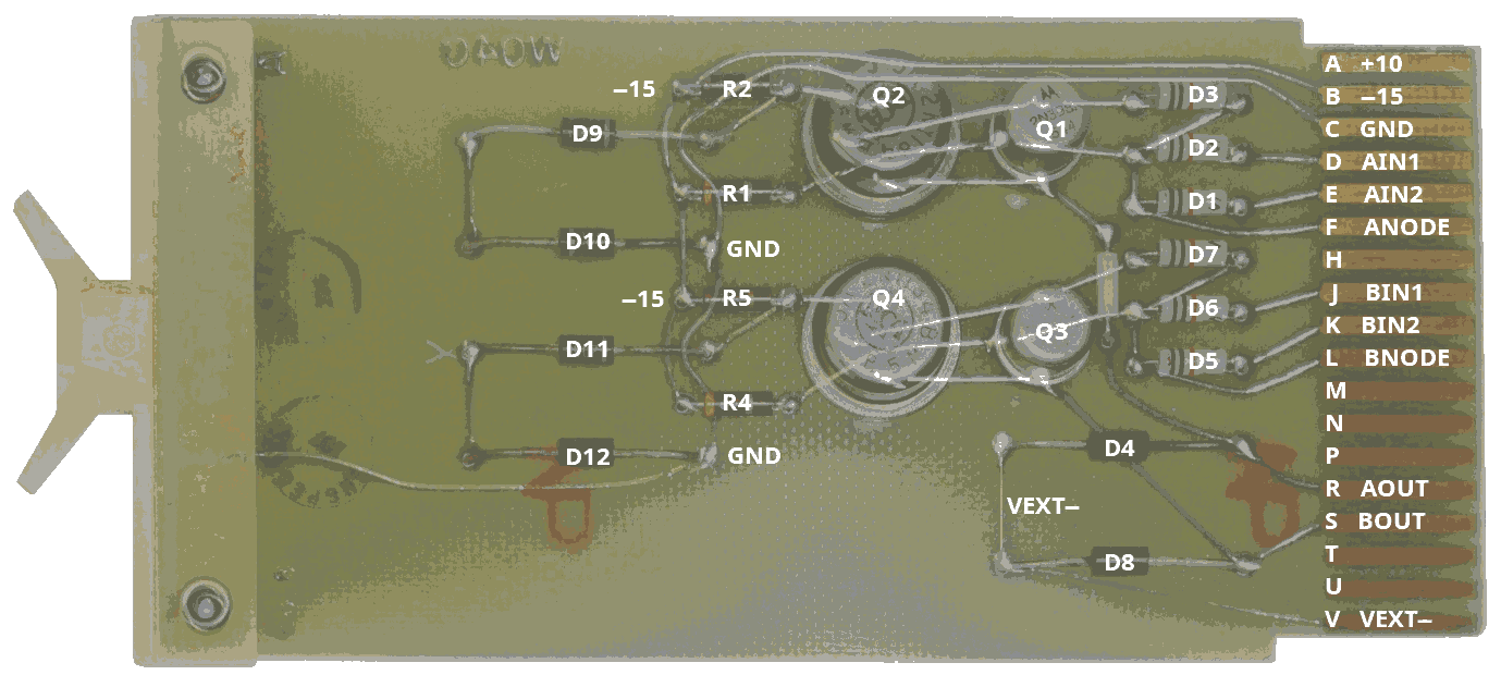
| W040A top | |
|---|---|
W040A bottom
| |
Bug 77: With Teletype output working, we wrote a test program to echo Teletype keyboard input to the Teletype printer:
6400 6031 A:      KSF             / loop top, skip if TTY keyboard ready
6401 5200         JMP     A       / polling loop waiting for input
6402 6036         KRB             / read keyboard into AC
6403 6046         TLS             / send AC to TTY
6404 6041 B:      TSF             / skip if TTY done
6405 5204         JMP     B       / polling loop waiting for output
6406 5200         JMP     A       / end loop, try for the next character
This program worked somewhat, it waited for keyboard input and echoed something to the printer, but rarely a printing character and never anything related to the key we pressed. The contents of the accumulator while the program awaits input should be the most recent character types, but was usually ither zero or all ones.
|
| TTY input data and sample clock |
|---|
|
| TTY input data and In Last Unit |
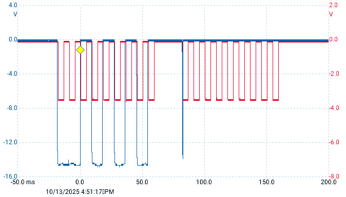
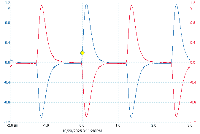
Looking at MF21R, the sample clock input to the pulse amplifier that drives the receiver shift register, we saw the expected 8 clock pulses triggered by the start bit, but we also saw a second train of clock pulses following the data. We see the same problem when we look at MF24E, a signal called In Last Unit that counts off the data bits.
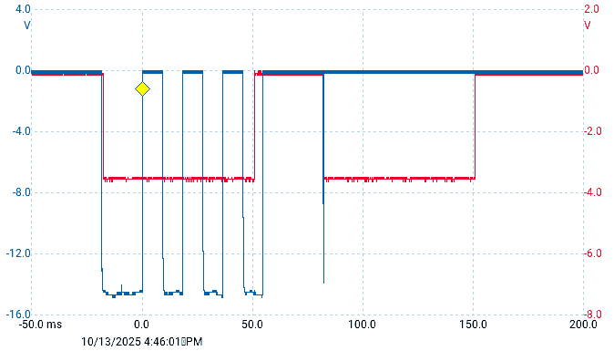
The scope traces shown here all show the received data when the '*' key is pressed, with the binary code 0101010. Our teletype adds an 8th bit which is always 1, so this is sent as 10101010, and the asynch data format sends the least significant bit first, prefixed with a 0, the start bit, and suffixed with 11, two stop bits, giving 00101010111 as the 11 units of the code. This is easy to see in the traces shown here.
Bug 52:
We immediately noticed the glitch at the end of the two stop bits.
While this is much shorter than the bit time of the Teletype, it is
definitely long enouth to trigger a second receive cycle. Since this
glitch appears in the data from the Teletype, it tells us that the Teletype
needs adjusting.
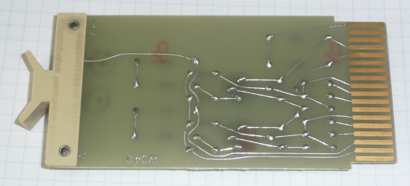
| |
| W040A layout | |
|---|---|
W040A schematic
| |
Bug 74:
Having worked out the schematic for the W040A, we could see that the
bad diode we found on Oct. 9
was in the current path to the solenoid driver, so it must be able
to withstand 0.6A and 70V. It appears to be used for its forward voltage
drop, with a bias resistor guaranteeing that about 0.01A will flow
through it when the driver is turned off.
The 1N4002 diode can handle 1A at 100V, so this seems to be a sensible
replacement.
Bug 52: On Oct 13 we noted that the Teletype was producing a glitch on the data line at the end of the stop bits. The Teletype keyboard produces parallel data; this data is converted to serial form by a distributor in the right rear of the typing unit. This has a carbon brush that sweeps around electrical contacts for each bit of data. We hypothesized that the glitch was caused by the distributor stopping precariously close to the end of the contact area for the stop bit, briefly breaking the connection.
Looking at the Teletype distributor adjustment instructions We found that, indeed, our distributor was a few degrees out of adjustment. Instead of pointing at the locating mark, the pointer on the distributor brush holder was pointing just beyound it. It was just barely possible to loosen the distributor mounting screw without disassembling the Teletype, and with repeated trials, we finally got the distributor adjusted. The problem was that tightening the mounting screw invariably moved the pointer, so we had to set the pointer somewhat back before tightening the screw to get it to end up correct.
It is interesting to ask why the glitches from the mis-adjusted distributor had no impact on the Teletype when operating in local mode. We suspect that they were simply too short to be noticed by the electromechanical serial-to-parallel data receiver in the Teletype.
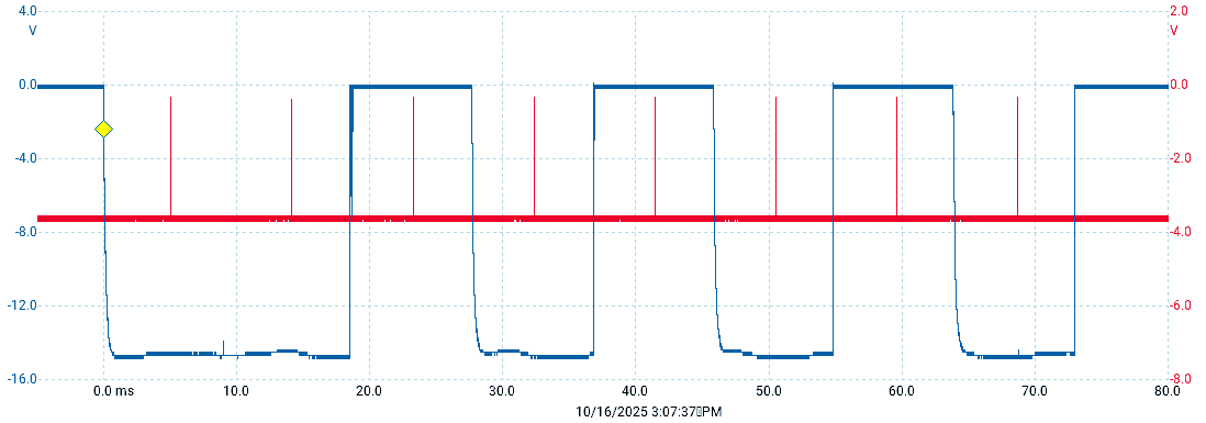
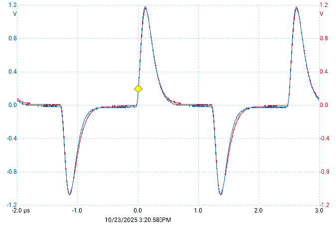
|
| TTY input data and clock |
|---|
|
| TTY input data and shift-register contents |
We then looked at the output of bit 0 of the teletype in shift register (pin MF22N). Drawing BS-D-8P-0-5 (page 10-45 of the Maintenance Manual) indicates that the shift-register is made of pulse-triggered flipflops. The DC clear input of all of these flipflops is pulsed used when input-acitve is asserted, but these flipflops should be not change at any other time. As the second trace to the right shows, the first bit of the shift register was being changed by every negative going edge of the input data. This is clearly wrong.
This led us to pull the R220 3-bit shift register board from backplane slot MF22. Even though we had just tested all the diodes, careful testing revealed that 3 more diodes on this board were bad. We suspect that the nearly random placement of diodes on this very crowded board led us to miss some of the bad diodes.
After these diodes were replaced, the Teltype worked with our test program.
Every character we typed on the keyboard was correctly echoed on the printer!
Bug 68: We anticipated the need for several 3-way backplane shorting jumpers, so we made them to match the 2-way jumpers we'd manufactured when we made safer groun clips for the scope.
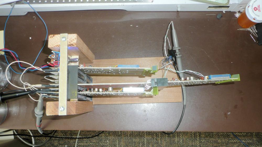
|
| Sense amplifier test rig |
|---|
We built the test rig shown here to compare boards A and I. It is basically the same rig we used on July 3, but with two G007 boards at the bottom in the photo linked to the G008 Master Slice Control at the top in the photo. One G007 is on an extender so the foil sides of both boards are accessible, and we used our 3-winding pulse transformer to connect the signal generator on the scope to the two sense amplifier inputs. We checked to make sure that the transformer windings were indeed giving identical outputs by switching which winding fed which sense amplifier.
|
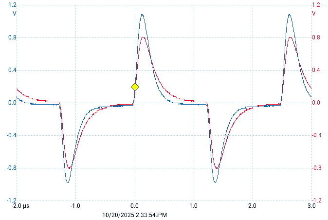
| Pin E on boards I (blue) and A (red) |
|---|
|
| The same after replacing Q2 |
Looking deeper into the differential amplifier we noted that the same gain difference was present on the output of the first stage. This led us to suspect that Q2 might have a lower gain than needed. Q2 is a matched transis, the matched transistor pair at the heart of that stage. DEC specifies an SDA-6 transistor, which they say is equivalent to a 2N2060. We have some of these on hand, so we replaced Q2 on board I.
This made a small difference in the gain, increasing the output by perhaps 5%. Given the way the threshold circuit works, this could actually be significant, but we had hoped for better.
And then, while clearing up the lab after making these measurements, we
realized our mistake. The two scope probes we were using were not identical.
Reading the fine print on the probes, the one we were using for the red channel
in the above scope traces was only rated to a few MHz, too close to our
operating frequency, and therefore, it is highly likely that that probe was
significantly attenuating the signal.
|
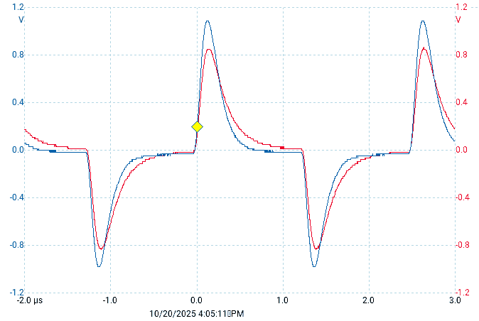
| Pins E and F on board I, balanced |
|---|
|
| Pin F on boards I (blue) and A (red) |
First, we re-balanced the differential amplifier on board A. Outputs E (blue) and and F (red) are complementary, as expected for a differental amplifier, and with identical scope leads, it was not difficult to balance the amplifier so they had identical amplitudes.
We then compared board A, with our replaced transistor pair Q2, with board I. The comparisons of pins E and pins F were indistinguishable, so we only show the result for pin F here. What is noteworthy is that the red and blue traces overlap so closely that they might as well be a single scope trace. There might be a 20mV difference, with board I slightly stronger. This is enough smaller than the amount the improved when we replaced Q2 that we suspect that board A is now far closer to the typical gain of our other G007 boards.
When we reassembled the machine, it worked for some simple tests, but
the chase light demo failed. Closer inspection showed that we are having
difficulty shifting data into the link bit from either direction. This
will be the subject of our next work session.
Bug 74: We ended work on Oct 23 having discovered that we could not shift ones into the link bit from either direction. DEC's drawing BS-B-8P-0-2 (page 10-29 of the Maintenance Manual) shows that the link bit and all of the data paths into it are handled on the R210 board in backplane slots in PA6 and PB6. We had scanned the diodes on this board in 2015, and replaced one diode then. We rescanned the diodes on this board and found another bad one (D41). While we are unsure how this diode could interfere with the data path we had trouble with, we replaced it and this fixed the problem.
We finished scannig diodes in row C of the multifunction I/O device backplane, that we started on Oct. 9. We found another bad diode. Row D remains to be done.
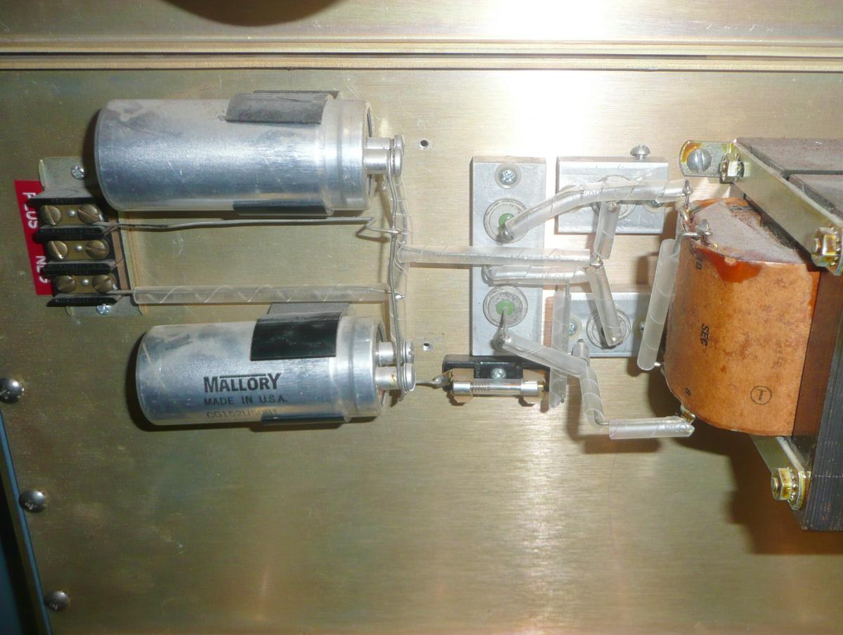
Bug 10: We set up to begin reforming the capacitors in the homebrew reader-punch power supply. In preparation for this, we disconnected the remains of the old wiring from this supply to the interfaces for the high speed paper tape reader and punch. This creates Bug 79.
Bug 43: We continued testing the PDP-8; to verify that we can shift left and right into the link bit, we used a very simple test:
0040 7604         CLA OSR         / AC = switches
0041 7010 A,      RAR             / rotate right (or RAL 7004 rotate left)
0042 5041         JMP     A       / iterate
In single-instruction mode, this allows you to set any pattern of bits in AC and then shift it left or right. Having verified that this works, we went back to this chase light program:
0000 7320         CLA CLL CML     / AC = 0, L = 1 (or 7301 CLA CLL IAC /AC = 1)
0001 2011 A,      ISZ     X       / outer loop, delay loop 1
0002 5001         JMP     A       /   iterate
0003 2011 B,      ISZ     X       /   delay loop 2
0004 5003         JMP     B       /   iterate
0005 2011 C,      ISZ     X       /   delay loop 3
0006 5005         JMP     C       /   iterate
0007 7010         RAR             /   rotate right (or RAL 7004 rotate left)
0010 5001         JMP     A       / iterate
0011 5001 X,      .-.             / iterate
This worked; it had failed earlier, leading to our search for a bad diode. Our next experiment involved subroutines; initially, this little program behaved strangely:
0060 4063 L,      JMS     S       / call S
0061 5060         JMP     L       / iterate
0062 0000 S,      .-.             / entry point, return address
0063 5462         JMP I   S       / return
When we ran this program, it jumped to location zero, our chase light program. Eventually, we figured out that the JMS was decoding as ISZ, incrementing location S until it was zero, then skipping the JMP, running the zero in location S as an and instruction, and then jumping indirect through S, which was still zero, and so taking the CPU to the chase light program.
Then, mysteriously, the problem went away and the program began working. This led us to try a more elaborate program with subroutines:
0200 4203 L,      JMS     S       / call S
0201 5200         JMP     L       / iterate
0202 7402         HLT             / halt to catch JMS converted to ISZ
0203 0000 S,      .-.             / entry point
0204 2213 S1,     ISZ     X       / delay loop 1
0205 5204         JMP     S1      / iterate
0206 2213 S2,     ISZ     X       / delay loop 2
0207 5206         JMP     S2      / iterate
0210 7001         IAC             / count in AC
0211 5603         JMP I   S       / return
0212 7402         HLT             / halt to catch possible strangeness
0213 0000 X,      .-.             / delay loop counter
We had trouble loading this in memory, but once properly loaded, it counted
in the accumulator. The next logical step is to try making the delay loop a
subroutine or nested loops, and also to try to make a program that reads
a string from the Teletype and echoes it on demand.
|
| Insulation added to wiring |
|---|
In preparation for the new wiring, we did some load calculations.
The total average load on the supply is therefore 4.15A, with a peak current of 9.1A. 18 AWG wire can handle this peak current, and 20 AWG wire is adequate for the average current. 20 AWG wire is, however, flimsy enough that we should use heaver wire for better mechanical strength.
While we were investigating power requirements, we also looked at the manuals to find the 120V loads of the devices:
Therefore, 120V power for the reader and punch takes a total of 3.6A, with a 9A starting surge for the punch. It is safe to assume that the starting surges for reader, punch and power supply will never overlap because the reader and punch have separate on-off switches and should be left off when not in use.
Until we find out how much 120V power the main cabinet can supply to the
second cabinet, we do not know if these can all be supplied under control of
the main on-off switch or whether a second wall plug will be required for the
reader and punch.
Bug 10: Over the duration of the afternoon work session, we turned up the variac providing AC power to the reader-punch supply until the supply was idling with an output voltage of 12.5V. We could not see any leakage at this level, but when we raised the output to 13V, we saw evidence of slow leakage. We will have to go slowly when raising the voltage from this point on.
Bug 10: We finished the work reforming the capacitors on the homebrew reader-punch power supply that we had started on Oct. 30. After reaching a no-load output of 37V, we let it idle at that voltage for an hour before turning the input voltage down so we could test the supply under load.
The dummy load we built on Aug. 11, 2014 for testing the main PDP-8 power supply has numerous 5Ω 50W resistors wired to a common bus, wired in parallel groups of 1, 2 and 3 resistors. We used connections for a group of 2 in series with 1 to make a 7.5Ω test load.
With the input set to 110VAC RMS, the no-load output voltage was 33V DC. Connecting the 7.5Ω load, the output dropped to 26.5V. We ran the test until we noticed one of the 50Ω 50W resistors smoking. At that point, we realized that we were dumping 62W into that resistor. (The test load includes 2 10Ω resistors that we could have wired in parallel to make a 5Ω 100W resistor.)
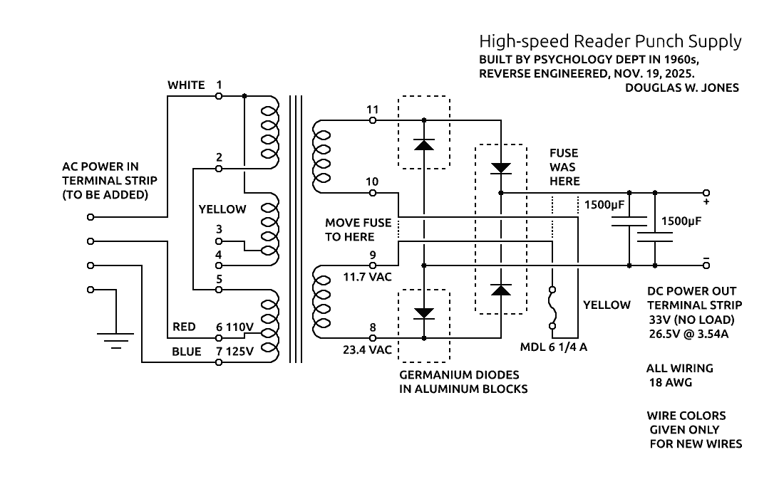
|
| Power supply wiring |
|---|
The 6.25A fuse in the supply is appropriate, given the peak average load of 4.15A we computed on Oct. 30. The fuse positon in the circuit is not optimal, because it does not protect against one of the rectifier diodes short circuiting. These diodes are huge and have a low enough forward voltage drop that we suspect they are germanium. (we cannot read their part numbers without disassembling them from the aluminum bricks that serve as heat-sink clamps.)
So, we propose to move the fuse to the AC side of the rectifiers. We can do this with minimal disturbance to the original wires by putting the fuse across the bridge that connects the two transformer secondaries in series.
The power cord for this supply is directly soldered to the primary windings of the transformer, the jumper that connects two transformer windings in series is uninsulated, and there is nothing protecting the many taps on the primary from accidental contact. Tap 4 on the transformer is at about 200VAC, well above line voltage. This is unsafe.
We propose to add a new terminal strip to the supply with the same kind of protection that DEC used on all of their 110V AC terminal strips, a fiberglass lid over the strip. We also propose to add an aluminum shield that limits physical access to the 110V wiring, again, following the model set by DEC's power supplies.
Bug 74: We decided to scan all of the diodes in the R210 boards boards in rows PA1 and PA2 of the PDP-8. In the process, we found one bad diode, but we also found that there are two versions of the R210 that have the same revision numbers and apparently the exact same layout. On the boards with 1966 date etched on them, jumpers replace 2 of the diodes present on the boards dated 1965. There is no evidence of rework on any of these jumpers, so we conclude that DEC discovered that two of their diodes were unnecessary and substituted jumpers. We almost replaced these jumpers with diodes before we reached this conclusion.
Bug 16 and bug 79: As originally built, the homebrew reader-punch power supply had a 3-prong power cord that plugged into a wall outlet independently from the rack wiring. This seems wrong, unless wiring it into the internal wiring would overload something. This lead us to attempt a complete analysis of the power requirements of the whole system, building on the preliminary work we did on Nov. 3.
| Amps@120V | Component | Source |
|---|---|---|
| 7.5A | basic PDP8 | Page 7-2 of the Maintenance Manual |
| 1.98A | Type 779 Supply | Page 124 of System Modules C-100, 1968 |
| 7.5A@10V from supply 1 = 75W
8.5A@15V from supply 2 = 127W total power = 202W @ 85% efficiency, 240W @ 120V this requires 1.98A | ||
| 1.84A | homebrew supply | schematic |
| 6.25A@30V = 187W
@ 85% efficiency, 221W @ 120V this requires 1.84A | ||
| 0.4A | Tally 424 reader | page 2 of Tally 424 Manual |
| 11.72A | Total, rack mounted | |
| 2A | BRPE punch | page 1-8 of BRPE Technical Manual |
| 4A | Teletype Model 33 | Label on back by power cord |
| 17.72A | Total | |
Note that the Type 834 Power Control Panel on the back of the PDP-8 rack contains a mercury contactor rated at 60A at 115V, but the current is limited by a 20A circuit breaker. Therefore, in theory, the entire load of the PDP-8 and peripherals can be controlled through this power control panel.
However, it may be better to power the external peripherals, the BRPE punch and Teletype Model 33, separately, perhaps using an external power strip with its own on-off switch and circuit breaker. This would keep the total power from each wall outlet below 15A.
Note that many kitchen appliances such as microwave ovens, toaster ovens and food processors draw from 10A to 15A at 120VAC. The entire system does not draw an outrageous amount of power, by this standard.
Note that we have ignored several things: