
The University of Iowa's DEC PDP-8Restoration Log
Part of
the UI-8 pages
|
The University of Iowa's DEC PDP-8Restoration Log
Part of
the UI-8 pages
|
This is a chronological log of the progress restoring the University of Iowa's PDP-8 computer. Entries are added at the end as work progresses. Click on any thumbnail image to see full-sized image.
|
| Plans |
|---|
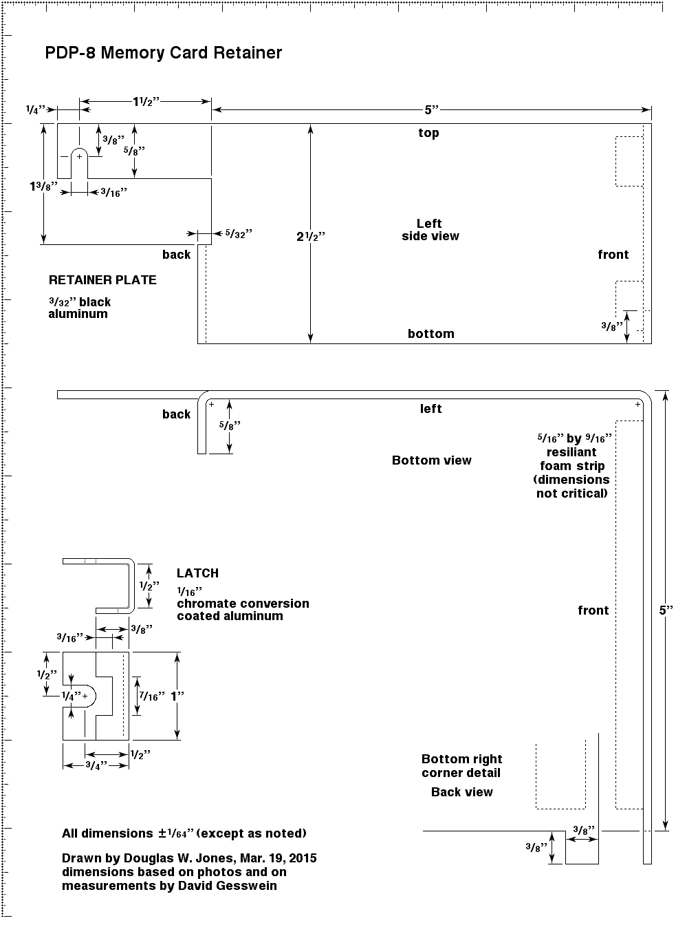
I measured the brackets, using our PDP-8 for comparison, and then sent the
resulting drawings to David Gesswein, who checked my dimensions against his
brackets and offered many (mostly small) corrections. The drawings given
here should allow us to make a bracket that is a reasonable duplicate of
DEC's original, although as with all parts that involve foam, we will need to
replace the polyurethane foam used with DEC's original brackets with something
equally resiliant but less prone to decay.
|
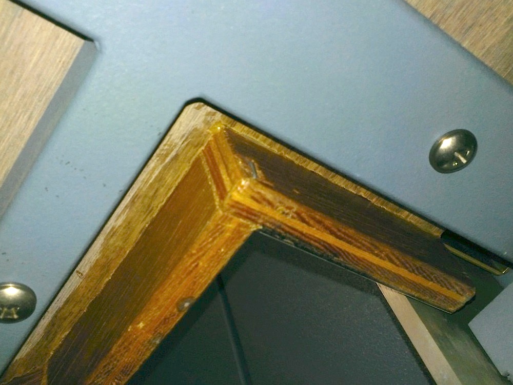
| Table detail. |
|---|
|
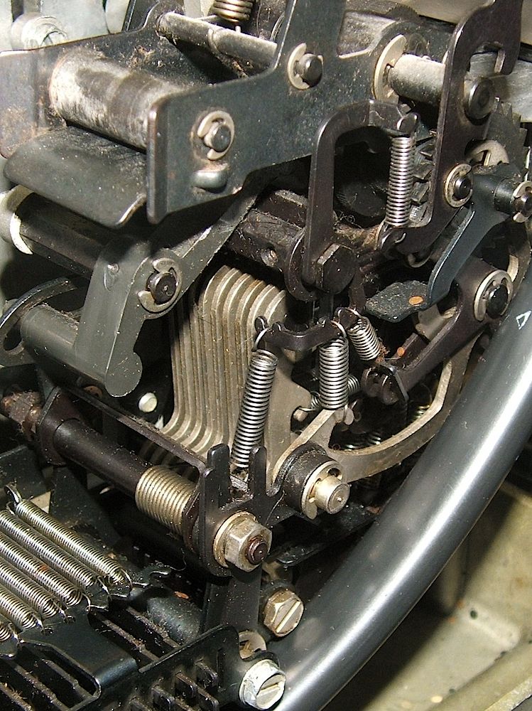
| The wrong spring! |
|---|
Unfortunately, as the bulletin documents, there were two versions of this design, an early design with a coil spring (not unlike the mystery spring we found) connecting the stripper bail to a hook above, and one using a torsion spring wound around the stripper bail mountin post pushing up on the bail from below. It was only after we mounted the mystery spring in the space between the bail and the hook above that we noticed that the torsion spring was present below the bail. In the photo, our extra spring is shown in the center of the photo (the leftmost of the three springs hanging from the lower extension of the hook), and the torsion spring pushing up on the stripper bail is visible below it (wrapped around the bail post).
As we were leaving for the day, we found a second location for a missing spring, the trip-lever spring on the selector clutch. We must move our extra spring to that location from where we misinstalled it.
We also managed to reassemble the keyboard correctly, so far as we can tell. Our prevous reassembly efforts had left the repeat key with nothing to do; it turned out that the nonrepeat lever and latch levers, while both present, had become hung up on the wrong side of the Universal lever, so were not operative and unable to engage with the repeat key. We think we have these in their proper places now, but it is very difficult to see how they engage and they are impossible to photograph. This is documented here:
|
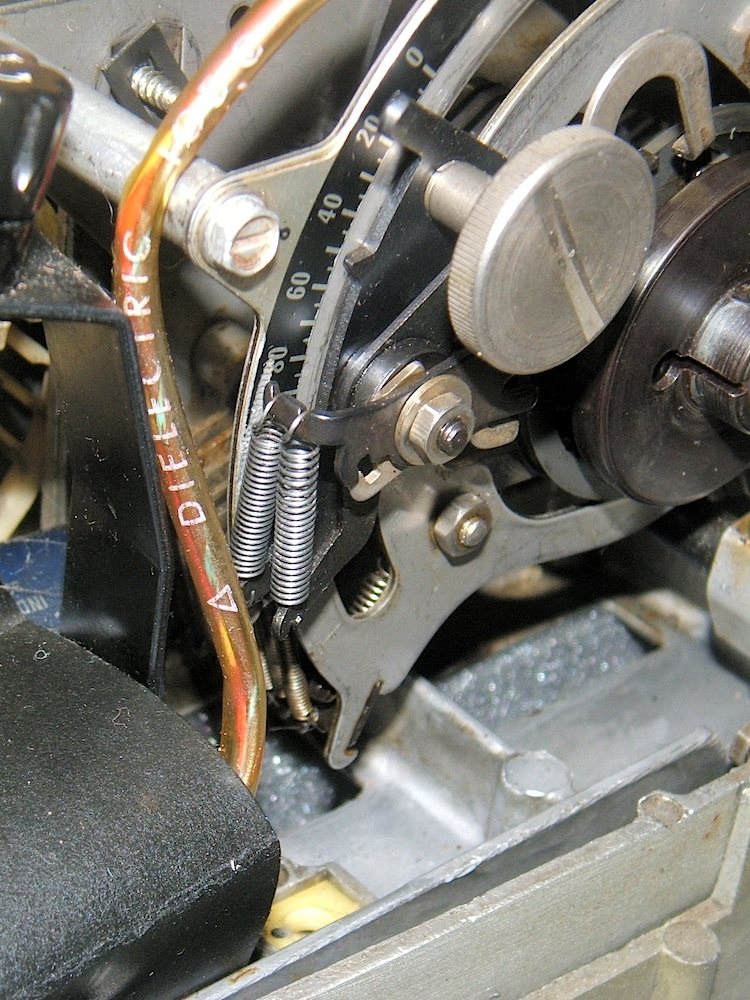
| The right spring! |
|---|
|
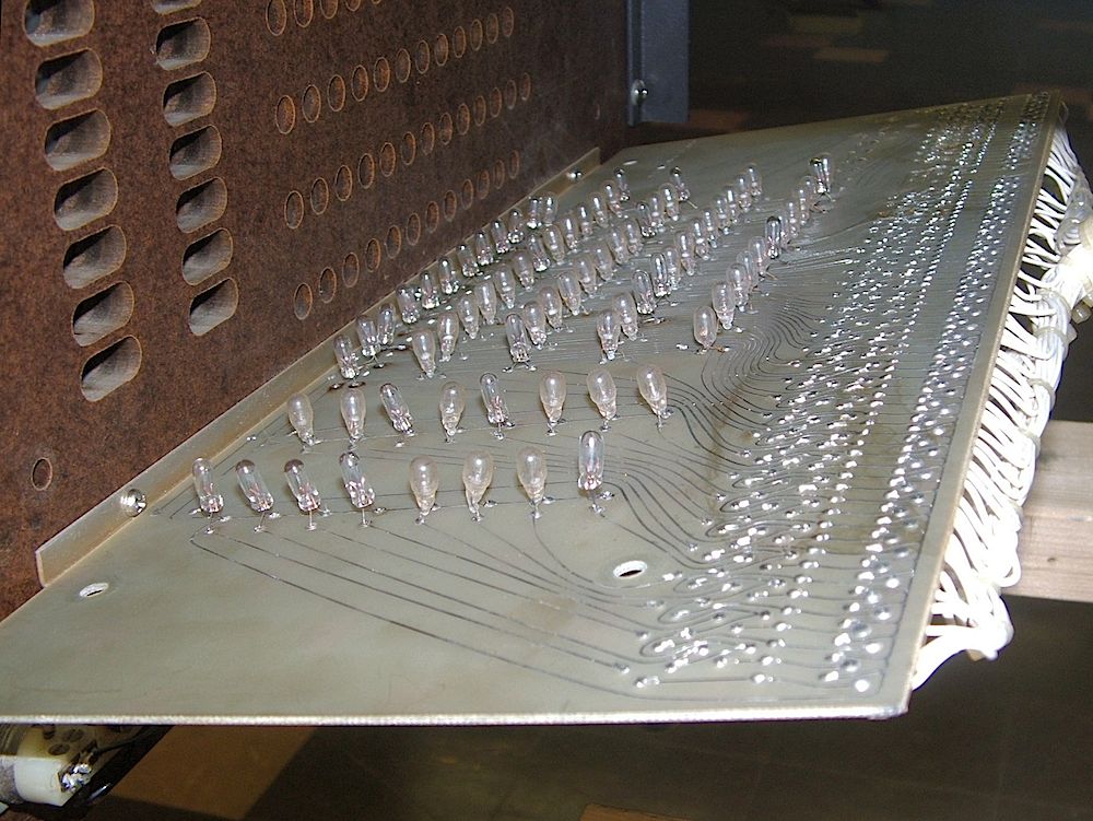
| The circuit board |
|---|
In order to diagnose the fault and do the necessary
repair, I pulled the circuit board from the back of the front panel.
The first time we pulled this board, we probably broke the leads for
several of the lamps on the bottom row (the Multiplier Quotient register).
Since then, we have learned how to replace lamps without removing the
circuit board from the masonite body of the front panel, but access to the
transistor and pull-down resistor requires pulling the board. As shown
in the photo, I pulled the board by tipping is back while the lower rear
edge of the board rested on the top edge of the rail holding the
switches. Before tilting the board back, I unscrewed the cable clamps
holding the wire harness to the chassis, so that the wire harness had
sufficient slack to follow the board down and support it in its lowered
position. This gives us full access to the solder side and component
side of the board.
|
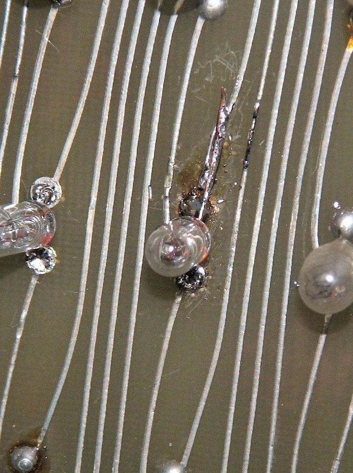
| The circuit board |
|---|
We note that DEC modules from the 1960s do not use a solder mask to limit soldering only to the component mounting pads. Instead, there is a uniform and fairly thick solder layer over all of the circuit traces. We hypothesize that this uniform solder layer served to bridge small defects in the etched copper circuit traces. In the photo to the left, you can see our repair, but you can also see, just to the right of the upper end of our repair, a spot where we heated the adjacent trace enough to melt the solder there, exposing what appears to be a small flaw in the etch. We need to test this before attempting to reassemble the front panel.
We also discovered that we will have to remove the masonite front panel
body from the computer in order to reassemble everything. DEC did not
design this front panel for easy maintainability.
|
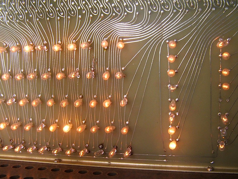
|
| Pre and post assembly tests | |
|---|---|
As you can see in the left photo above, the MA9 lamp now works. Unfortunately, removing the panel seems to have damaged at least two other lamps that used to work.
Bug 46: We have learned a lesson here: Taking shortcuts with the front panel does not pay because the lamp wires are so delecate. If you need to open up the front panel, remove the glass, then get a 3/4 inch thick board to support the face of the panel so it doesn't rest on the switches, then lower the whole assembly face down onto the table top (even an improvised table will suffice), and only then loosen the screws holding the circuit board. Lift the circuit board straight up to remove it from the (face down) masonite front panel body, and don't even touch the lamps while it is extracted. To reinstall the circuit board, tip it straight down and then lower slowly, again, trying to minimize all contact between the lamps and anything. All lamp replacement should be done with the circuit board mounted on the masonite body so that the masonite protects the lamps that aren't being replaced.
After reassembling the front panel, we repeated the lamp test, and flagged
the three lamps that do not light with stickers. Replacement and testing of
these will have to wait for another day.
|
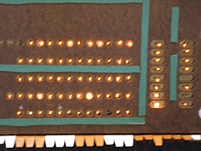
| All lamps lit! |
|---|
Bug 46: Of course, the lights did not all come on, but when I touched the two that did not, they came on. The problem appears to be cold solder joints, so I re-soldered those lamps, tested again, and then put the glass faceplate on the front panel and tested again before taking the photo shown here.
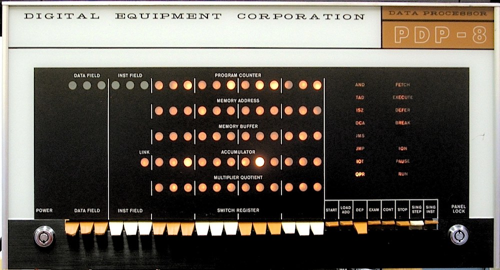
Note: The DATA FIELD and INST FIELD lights
do not light because this PDP-8 was purchased without the Memory Extension
Control option, and no lamps are installed behind these two 3-bit displays.
Bug 43: With the front panel lights all working, I resumed testing of the function of the PDP-8. Before powering it up, I checked that all the margnial check switches were in the normal (not the test) position and that all the wiring that had been disconnected for front panel work was reconnected. With that taken care of, I powered up the machine and performed the following tests:
The next thing to test is the switch register and the ability to set the program counter from the switches. The following table shows the values set on the switch register and the values observed in the program counter after pressing the momentary load address switch:
| Switch Register | Program Counter | |
|---|---|---|
| 0000 | 0000 | |
| 7777 | 7763 | |
| 0000 | 0000 | |
| 7777 | 7363 | |
| 0000 | 0000 | |
| 5252 | 5242 | |
| 2525 | 2121 |
Also note: The load address switch did not always work. Sometimes, it took several presses of this switch to get the computer to react. We need to find out why.
I turned off the computer and I looked at the processor map in the CPU maintenance manual to find out what boards hold what bits of the program counter. I then swapped the boards that hold bits 3 and 8 with the boards that hold bits 10 and 11, trying to put all the bad bits at the bottom of the program counter.
Powering up the machine and repeating these tests, swapping boards had no impact. Therefore, problem must be in the path from the switches to these boards, while the boards themselves are probably good. The problem could be as simple as bad electrical connections to the switches.
Pressing examine transfers the program counter to
the memory address register before it increments the program counter.
As a result, these tests also tested that register.
Bit 0 (the most significant bit) of the memory address register appears
to be stuck on (1).
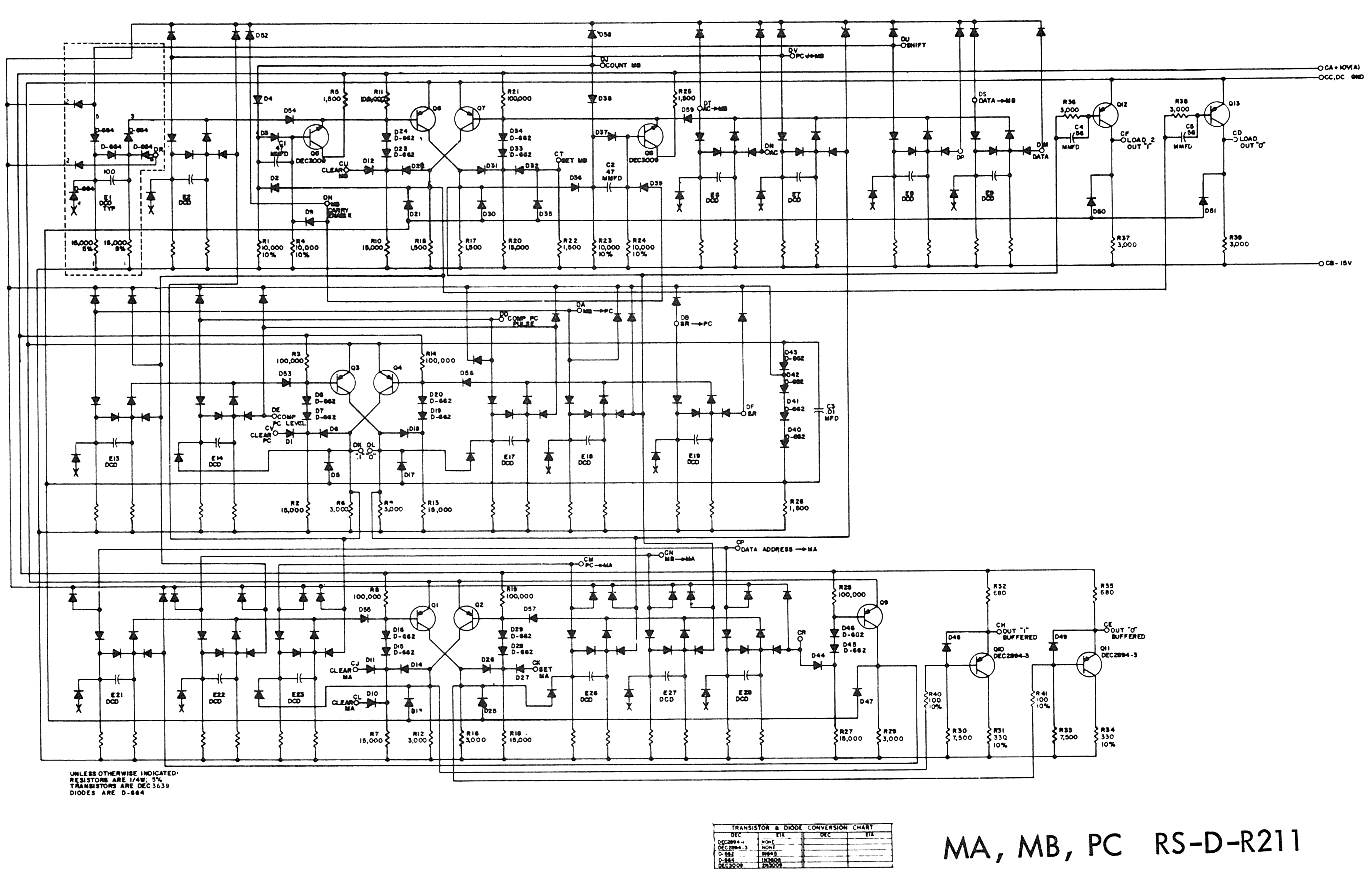
Bug 43: Continuing the testing from April 21, Zimu Zhang and I investigated the wiring between the switch register and the R211 boards holding the bits of the program counter. As it turns out, each switch is directly wired to pin DF of the corresponding R211 board. The board itself is documented in Maintenance Manual Drawing RS-D-R211 MA, MB, PC. The wiring of the switch-register to the program counter and memory address register is documented in Maintenance Manual Drawing BS-D-8P-0-4 PC and MA Registers.
With an ohm meter, we determined that lifting each switch connects pin DF of the corresponding R211 board to the ground bus soldered to the back of the switch register through one of the 100Ω resistors on the W026 boards that connect the front panel lights and switches to the backplane at backplane positions PA4 and PB4. Most of the switches reliably grounded the corresponding pin DF when raised, but the switches for bits 3, 8 and 9 were not reliable. The problem appears to be in the switches themselves. The problem became less severe with repeated toggling, so we suspect that getting a bit of oil (grease solvent) into the switches will alleviate the problem. If that does not work, we may have to disassemble and clean these switches the way we did the Marginal Check switches in our response to Bug 44.
On April 21, I noted that bit 0 (the most significant bit) of the memory address register is stuck on. To diagnose this problem, we exchanged the R211 board in slots PC7 and PD7 with the board in PC8 and PD8 (these are double-high boards). These boards hold bits 0 and 1 of the PC, MA and MD registers.
We then turned on the machine and repeated the basic front panel tests.
Exchanging the boards moved the bad bit from bit 0 to bit 1, so we now know
that the R211 board in slot PC8-PD8 has a problem. This creates
Bug 49.
|
|
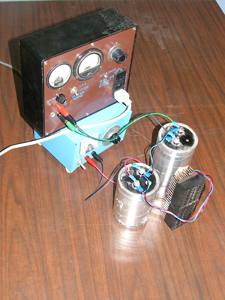
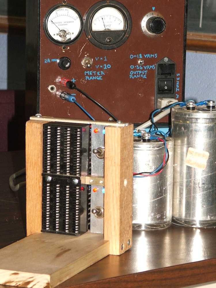
| The board-level test rig. | |
|---|---|
Bug 49: After verifying that the power supplies were adjusted for the correct voltages, I let the bleeder resistors pull the voltage down, and then plugged in the questionable R211 board, powered everything up, and began exploring it with a voltmeter. The initial focus of this exploration was on the MA (memory address) flipflop (Q4 and Q6), its output buffers (Q10 and Q11), the buffered MA outputs (pins CD and CH), and its set (pin CK) and reset (pins CJ and CL) inputs. This is an extraordinarily complex circuit board by the standards of the time, with a component density much higher than most other boards in the machine. As a result, merely relating the components on the board to those on the R211 schematic diagram in the maintenance manual was time consuming.
While I was just starting to experiment, I began to smell hot electronics,
so I turned off the power and quickly scanned the board for hot spots
using my thumb. A pair of transistors other than the ones I had been
focusing was quite warm. It will take some time to relate those to the
schematic diagram, so this work will have to wait for some other day.
|
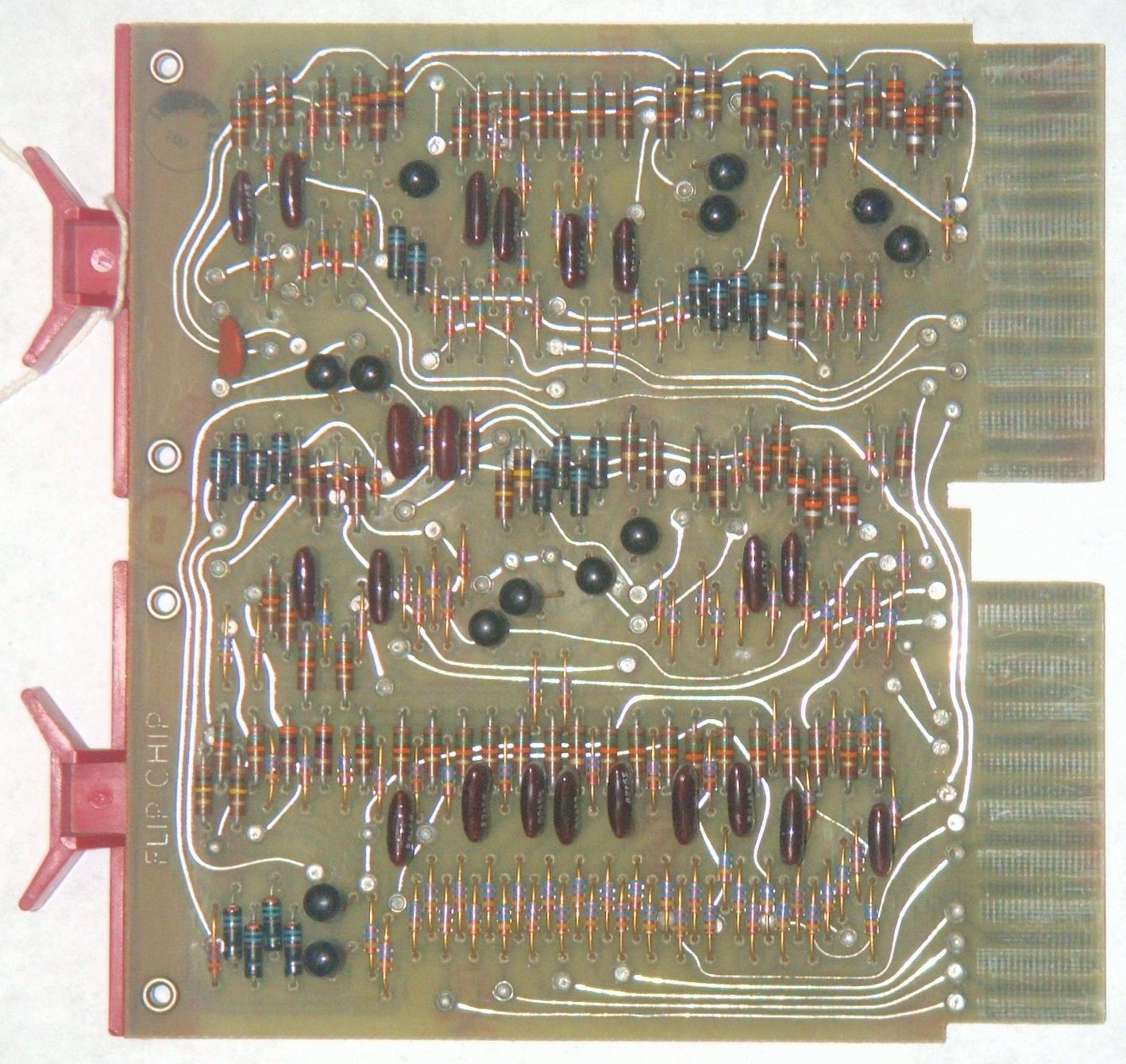
|
| The R211 board, top and bottom. | |
|---|---|
|
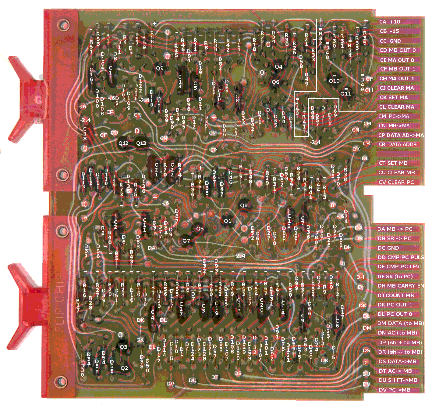
| R211 reverse engineered. |
|---|
The Preliminary Maintenance Manaual (F-87P2, copyright 1965) shows a schematic diagram on the top half of page 10-12. This schematic diagram has only scattered part numbers, but the area around the memory address output buffers is fully numbered and corresponds to our circuit boards.
The image showing the result of the reverse engineering shows both sides of the board, superimposed (with traces on the solder-side shaded red). The text gives:
Bug 49:
In the process of reverse engineering, I discovered
the reason for the hot electronics smell I noted on
May. 19.
The R211 board has non-standard wiring on pins DA and DB (pins A and B of
the lower card-edge connector). These are used as data inputs, so plugging
this board into a generic backplane that has pin A of every connector wired
to +10 and pin B of every connector wired to –15 will cause trouble.
We need to investigate what we might have burned out by applying power supply
voltages to these two inputs. The most likely victims are the diodes that
clamp the inputs within the -3V to 0V range.
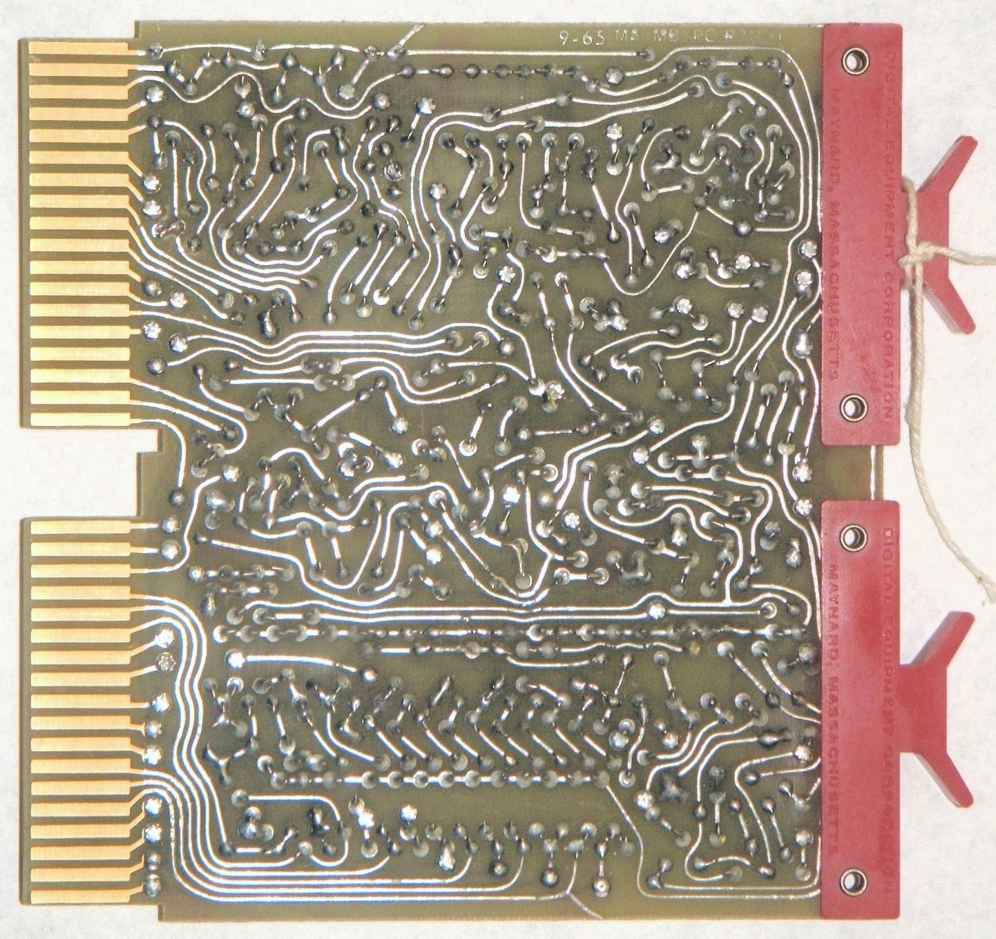
Bug 50: Vincent Slyngstad asked what the revision letter is on the R211 boards from our machine. The revision letter is totally illegible on the board we pulled, but when we pulled other boards from the machine, we found that all of them have the same revision data etched into the solder side of the board: "9-65 MA MB PC R211 H".
Neither edition of the maintenance manual lists revision numbers,
but as already noted, Vincent Slyngstad concluded that the
1966 schematic diagram
appears to match
his work
reverse engineering an R211 J board.
We now know that the
1965 schematic diagram
corresponds to the R211 H board.
|
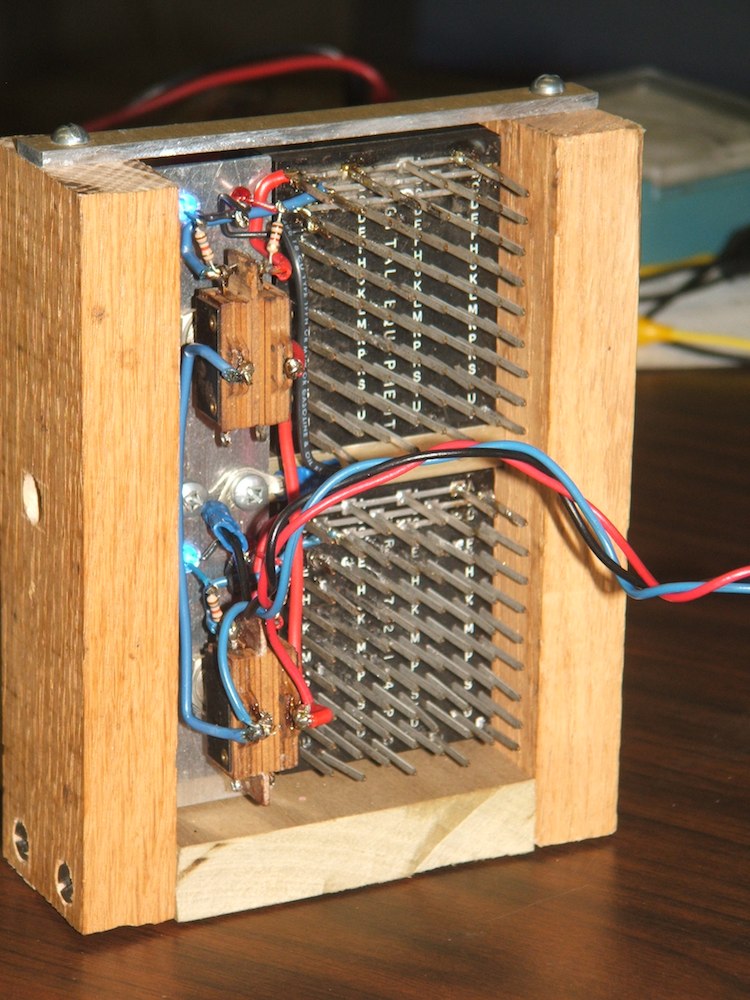
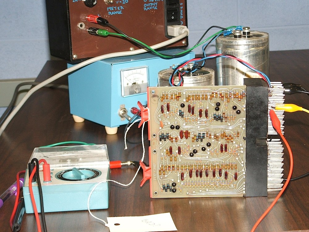
|
| The board test rig improved. | |
|---|---|
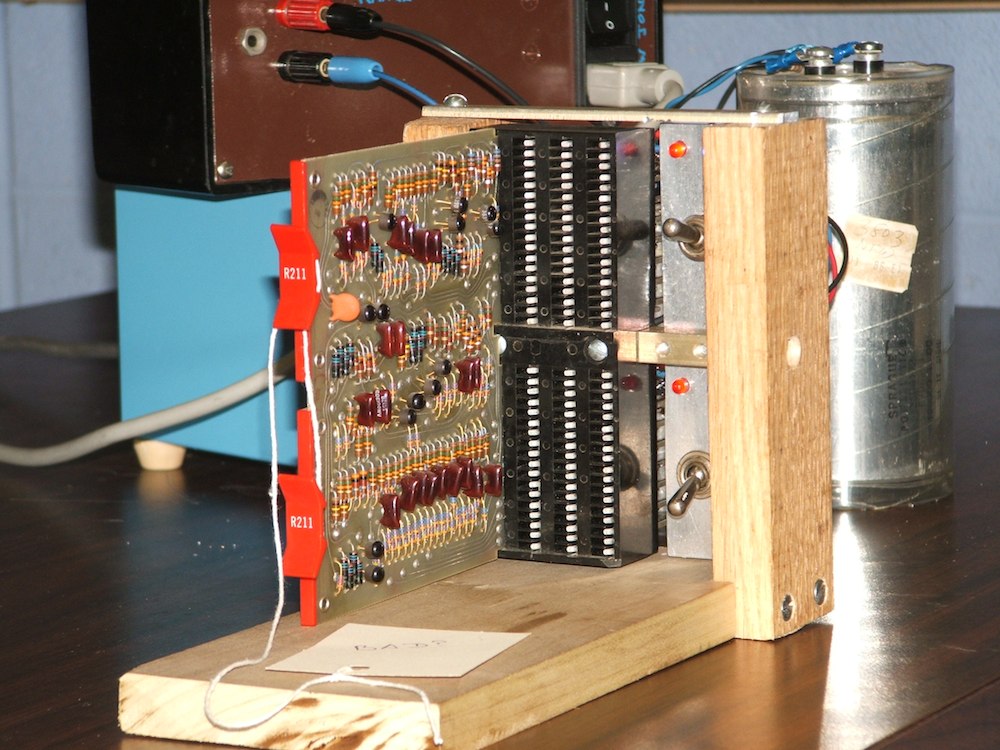
| |
| R211 board in test rig. | |
Bug 49: Having improved the test rig, I plugged in the R211 board and began poking around with a voltmeter. The first things I tested were the on-board -0.6V and -2.4V busses. These voltages are generated on board by a cascade of diodes (D110 to D113) and a series resistor (R54) (See the 1966 schematic diagram). Applying -15V to pin DB would have reversed biased the diodes D92 and D93 on the board. This is unlikely to have caused any damage (these are a DEC D-664 diodes, 1N3606, rated at 50V).
Applying +10V to pin DA is more problematic. This puts D91 and R47 in series across 25V. R47 is 15KΩ, so this pushes 1.6mA through D91. This is not a problem; the 1N3606 can handle 100mA. This also puts 25V across D84, D112, D111, D110 and R54. R54 is 1.5KΩ, and the forward voltage drops of the diodes reduce the voltage to about 23V, so this pushes 15mA through D84. Again, this is not a problem, being under 100mA. At this current, however, R54 is dissapating 0.35W, and it is a 1/4W resistor. That explains why the board started to smell of hot electronics! The loction of R54 on the board is in the vicinity where things seemed very hot when I scanned the board with my thumb after smelling hot electronics and turning off the power on May 19.