Trippy PTZ WebcamControl board programmer's manual, V 1.10
Part of
the Trippy web pages
Copyright © 1999, Basic Telepresence Inc., revised and corrected, 2022, Douglas W. Jones. |
Trippy PTZ WebcamControl board programmer's manual, V 1.10
Part of
the Trippy web pages
Copyright © 1999, Basic Telepresence Inc., revised and corrected, 2022, Douglas W. Jones. |
A programmer wishing to write code for the PIC on the Basic Telepresence Serial Trippy control board should get a copy of the Microchip PIC16C7X data sheet (1997)! This "sheet" runs 288 pages and covers all aspects of PIC programming and interfacing. This manual is organized as an appendix to the data sheet! In addition, the data sheet for the Microchip 24C32A EEPROM chip will be needed if the on-board EEPROM is to be used.
The purpose of a watchdog timer is to force a device reset if the software resident in the device does not reset the watchdog timer. This prevents the device from hanging, for example, because of transient electronic faults or programming errors such as infinite loops. The PIC has a watchdog timer with a very inaccurate period that is guaranteed to be longer than 7ms. In the prototype software, this timer is enabled and all code should reset the watchdog timer every 5ms. With the processor clocked at 16MHz (4 Million instructions per second), this allows 20K instruction cycles between resets!
With a 16MHz clock crystal the PIC executes 4 million instructions a second, and the internal clock source for the on-chip timers is 4MHz. The serial Trippy has no provisions for external clock sources. At this rate, 4 clock ticks is 1 microsecond and 4000 ticks is a millisecond. Deriving a 5KHz clock from the 4MHz clock, as suggested for PWM timing on the stepping motors, requires a clock period of 800 ticks. The 1:4 prescalers available on timers 0 and 2 allow this period, and so does the native resolution of Timer 1.
In the prototype software, timers 0 and 2 are disabled and timer 1 is configured as a 5Khz periodic clock using CCP module 1 to hold the period. When CCP module 1 finds TMR1 = CCPR1, it resets TMR1 and requests an interrupt. CCPR1 is initialized to 800 and held constant, the timer1 interrupt is never enabled, and the interrupts from CCP module 1 provide the software time-base used to generate step sequences in the motors.
If PWM output on RC5 is desired, this can be generated by using CCP module 2 to hold the cutoff (as a fractions of 800). In this case, interrupts from module 1 turn on RC5, and interrupts from module 2 turn it off. In the prototype code for the Serial Trippy, the CCP1 interrupt service routine takes about 10% of the CPU time, so PWM frequencies below 10% cannot be achieved.
Output bits RB0 through RB7 control the power to the two windings of each of two permenant magnet stepping motors. These are arranged as follows:
| Motor | Winding | Bit | Connection |
|---|---|---|---|
| 1 | 1 | RB0 | J2-1 |
| RB1 | J2-2 | ||
| 2 | RB2 | J2-3 | |
| RB3 | J2-4 | ||
| 2 | 1 | RB4 | J3-1 |
| RB5 | J3-2 | ||
| 2 | RB6 | J3-3 | |
| RB7 | J3-4 | ||
If the output bit is set to logical 1, the corresponding pin of the indicated jack will be held at +12 volts. If the output bit is set to logical 0, the corresponding pin will be held at ground.
Each motor winding is controlled identically by two bits. The states of the motor windings are as follows:
| RB0 | RB1 | Winding State |
|---|---|---|
| RB2 | RB3 | |
| RB4 | RB5 | |
| RB6 | RB7 | |
| 0 | 0 | Off low (slow decay) |
| 0 | 1 | Reverse |
| 1 | 0 | Forward |
| 1 | 1 | Off high (slow decay) |
Earlier versions of the board supported fast decay mode, where residual current in the motor windings flowed from ground to +12 through two of the on-chip diodes in the L293D motor driver.
In slow decay mode, residual current will recirculate through one closed switch and one diode working against the forward voltage drop of the switch, diode and motor winding.
The directions listed above for forward and reverse current flow are arbitrary. If a stepping motor is wired as follows:
| J2/J3 Pins | Motor Wire | Bit |
|---|---|---|
| 1 | black | RB0 RB4 |
| 2 | red | RB1 RB5 |
| 3 | blue | RB2 RB6 |
| 4 | green | RB3 RB7 |
The motor should rotate counterclockwise when the outputs are sequenced as shown in the following table:
| Data Bits | ||
|---|---|---|
| RB3-RB0 | motor on J2 | |
| RB7-RB4 | motor on J3 | |
| 0 0 0 0 | off | low power consumption |
| 1 1 1 1 | off | |
| 1 0 0 0 | step 1 | steps in counterclockwise order |
| 1 0 1 0 | step 1.5 | |
| 0 0 1 0 | step 2 | |
| 0 1 1 0 | step 2.5 | |
| 0 1 0 0 | step 3 | |
| 0 1 0 1 | step 3.5 | |
| 0 0 0 1 | step 4 | |
| 1 0 0 1 | step 4.5 | |
Cycling the outputs in step order, 1 2 3 4 1 2 3 4 will rotate the motor counterclockwise, when viewed from the top, while cycling the outputs in the opposite order will rotate the motor clockwise.
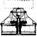
Viewed from the top, counterclockwise motor rotation turns the Trippy camera mount counterclockwise or inclines the camera downward (depending which motors are turning). One motor step translates to 0.25 degrees on the pan axis or 0.0625 degrees on the tilt axis. These figures assume a 7.5 degree per step motor with gear ratios on the rotate drive train of 12:60 and 16:96, and 4:1 bevel gears for the tilt mechanism. Because of backlash in the gear trains, the actual resolution achieved by the Trippy will generally be around one degree.
The above table allows for half-stepping! The whole-steps in the table refer to positions that are stable with the power off. The half-steps refer to intermediate motor positions that can be held with power on; the motors delivers their full rated torque only at these half-steps, but if power is turned off in these positions, the permanent magnets in the motors will tend to swing them to the nearest whole step.
Note that, in the motor off positions, the stepping motor windings are shorted. This causes a dynamic braking effect that will not hold the motor in a fixed position against a heavy load, but will offer resistance to any motion of that load and will damp oscillation in the mechanical system.
If PWM control of the current through a motor winding is desired, this can be accomplished by 5Khz alternation between 00 and either 01 or 10 outputs for that winding. The frequency 5Khz is suggested by the L293 data sheet. The prototype software does not use this mode.
It should be noted that the L293 has switching delays of about 1 microsecond, and a 5KHz frequency involves switching every 100 microseconds. Therefore, the suggested frequency puts the chip in transition about 1% of the time. We are running at 12V, 1/3 of the maximum voltage for this chip, so the power dissapated in switching transients should be cut by a factor of 3 or more. Therefore, we should be able to run in transistion 3% of the time, or use PWM frequencies of up to 15KHz. Use of such high frequencies should largely eliminate audible PWM hum in the motors.
The serial port, J4, is connected to the PIC asynchronous receiver-transmitter through a Maxim MAX243 interface chip. This chip serves to generate the voltages needed for RS232 signalling and convert the TTL compatable signals from the MAX243 chip into these levels.
J4 is wired to conform to the expected wiring of an 8-pin mini-DIN RS232 port. CTS, TxD, ground, RxD and RTS (pins 2, 3, 4, 5, 6) are fully supported, and DTR (pin 1) is minimally supported. Full EIA flow control is possible for outgoing data, while the Trippy always asserts that it is ready to receive data.
Serial input from J4 pin 5 (RxD) is routed through The R1 channel of the MAX243 chip to the RC7/RX input of the PIC. In the process, logic 1 is converted from anything below 0.8V (typically 0V to -15V) to 5V, and logic 0 is converted from anything above 2.4V (typically +5V to +15V) to 0V.
Serial output from the RC6/TX output of the PIC is routed through the T1 channel of the MAX243 chip to J4 pin 3 (TxD). In the process, logic 1 is converted from 5V to -10V, and logic 0 is converted from 0V to 10V.
The clear to send signal to the RC2 input of the PIC is routed through the R2 channel of the MAX243 chip from J4 pin 2 (CTS). In the process, logic 1 (not clear) is converted from anything below -1.4V (typically -5V to -15V) to 5V, and logic 0 (clear) is converted from anything above -0.2V (typically +5V to +15V, but also an open circuit) to 0V. The threshold for CTS allows the use of cables that do not support hardware flow-control.
The request to sent signal from the RC3 output of the PIC is routed through the T2 channel of the MAX243 chip to J4 pin 6 (RTS). In the process, logic 1 (no request) is converted from 5V to -10V, and logic 0 (request) is converted from 0V to 10V.
The data terminal ready output at J4 is asserted (held at 10V with a 1K series resistor) whenever logic power is available. RS232 client hardware may use this output to detect whether the Trippy is powered up, or this may be used to defeat hardware flow-control on the output channel from the client, indicating that the Trippy is always ready to accept client data.
It is important to note that the PIC is clocked at 16MHz when configuring the baud rate of the internal USART connected to pins RC6/TX and RC7/RX. Thus, the most likely baud rates are from 1200 Baud to 19.2 KBaud, using BRGH=0 mode. The prototype software uses 9600 baud.
The internal option port (J5) is wired as follows:
| J5 Pin | use |
|---|---|
| 1 | ground |
| 2 | RC1 |
| 3 | RC0 |
| 4 | +5V |
No on-board wiring commits RC0 and RC1 to input or output functions, but the most likely use for these signals is to connect to photosensors used to provide feedback on motor positions. In this case, RC1 and RC2 should be programmed as inputs.
The external option port (J6) is wired as follows:
| J6 Pin | use | |
|---|---|---|
| 1 | RA0 | |
| 2 | +12 | unregulated |
| 3 | +5 | |
| 4 | RA5 | |
| 5 | RA4 | |
| 6 | RA1 | |
| 7 | ground | |
| 8 | RA3 | |
| 9 | RA2 | |
No on-board wiring commits RA0 through RA5 to input or output functions. Pins RA0 through RA5, excluding RA4, are wired identically and may be safely used as either input or output. Pin RA4 should be used with care; see section 5.1 of the PIC manual for details.
A 2-wire I2C bus is connected to a Microchip 24LC32A 4K byte EEPROM chip, wired with the A0, A1 and A2 chip-select inputs set to 000 and the WP (write protect) input grounded (not protected).
Warning! The I2C bus is connected with the clock line attached to RC5 and not to RC3, so all I2C functions must be done in firmware, without use of any of the built-in I2C hardware. The SDA/RC4 line is used for I2C data, but because of the unconventional clocking, this must be viewed as a coincidence, and the I2C support hardware on the PIC must be disabled at all times.
The bulk of the above text is from my files. The original was a plain text document (.txt format), so in tranferring it to the web, I converted to HTML and took the time to correct various errors and bring the documentation of the different connectors up to comparable standards.
Note that Rev 1.11 was the final board revision, so the documentation here does not fully cover version used in the Trippy as it went to market.
I actually used this programmer's manual as an aid in developing the firmware. When a product gets as complex as the Trippy, you need a manual even for the parts you designed and built yourself. Also, the manual for each board was delivered to Basic Telepresence to help others who might want to repair my firmware or write their own to replace it.