14. The Memory Subsystem
Part of
22C:60, Computer Organization Notes
|
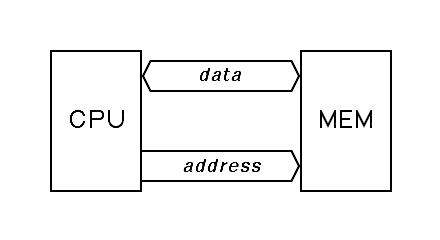
Up to this point, we have assumed a very simple model of main memory, where the address output by the processor goes straight to the memory without modification, and where the data path to and from memory is not interrupted by anything. An abstract view of this naive memory model is given in this figure.
|
|
There are two problems with this model. The first is one of speed! A typical central processor of the year 2000 can execute about 1 billion instructions per second, while typical memory of the year 2000 can handle only about 20 million memory references per second. Central processors are about 50 times faster than main memory!
First generation processors, those designed with vacuum tubes in 1950 or those designed with integrated circuits in 1965 or those designed as microprocessors in 1980 were generally about the same speed as main memory. On such processors, this naive model was perfectly reasonable. By 1970, however, transistorized supercomputers were being built where the central processor was significantly faster than the main memory, and by 1980, the difference had increased, although it took several decades for the performance difference to reach today's extreme.
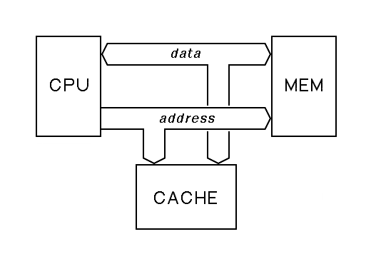
Our solution to this problem is to use what is called a cache memory between the central processor and the main memory. Cache memory takes advantage of the fact that, with any of the memory technologies available for the past half century, we have had a choice between building large but slow memories or small but fast memories. This was known as far back as 1946, when Berks, Goldstine and VonNeumann proposed the use of a memory hierarchy, with a few fast registers in the central processor at the top of the hierarchy, a large main memory in the middle, and a library of archival data, stored off-line, at the very bottom.
A cache memory sits between the central processor and the main memory. During any particular memory cycle, the cache checks the memory address being issued by the processor. If this address matches the address of one of the few memory locations held in the cache, the cache handles the memory cycle very quickly; this is called a cache hit. If the address does not, then the memory cycle must be satisfied far more slowly by the main memory; this is called a cache miss. All cache systems implement some policy to determine what small set of memory locations are held in the fast memory inside the cache and when this set will change. This is called the cache replacement policy.
|
A cache constantly monitors the data and address busses that connect the processor to the main memory. This requires that this bus be designed to allow such eavesdropping, and it requires that the memory be designed to allow a cache to preempt it, forcing the premature completion of a memory cycle that would otherwise take much longer.
Without cache memory, the applications programmer would have to explicitly transfer data between the large main memory and the small but fast cache. With a cache, this transfer is automated. It is natural to ask, can we automate the transfer of data between other levels in the memory hierarchy? The answer to this question is a firm yes. In 1962, Ferranti Ltd., working with Manchester University solved this problem with the introduction of the Atlas computer, the first computer to incorporate what was later called a paged memory management unit to support virtual memory.
By 1970, several other commercially available systems supported virtual memory and IBM was scrambling to support this on their mainframe computer systems. By 1985, several microcomputer-based virtual memory systems were being sold, and by 2000, virtual memory technology was universally available on all but the smallest embedded computer systems.
Put simply, virtual memory is present in any system where the memory addresses issued by the program are transformed, by any mechanism, to produce the memory addresses actually seen by the memory hardware. The mechanism that performs this transformation has come to be called a memory management unit.
|
Memory management units take the address issued by the central processor and replace it with some other address, allowing all of the parts of memory that the current program needs to be stored in a relatively small main memory, while unneeded parts of memory are stored on disk or some other larger, slower memory. So long as the program never trys to use the other memory, it runs at full speed, but when it issues an address for a word that is not currently in main memory, the memory management unit forces a trap, allowing the operating system to bring the required data into memory, an action that will probably involve moving other data from main memory to disk. This activity is called a page fault.
Where we spoke simply of the address of a word of data in memory, adding a memory management unit forces us to distinguish the address is used as input to the memory management unit from the address it produces as output. The address input to the memory management unit is the virtual addresses, while the memory management unit output is the physical addresses. The function of the memory management unit is therefore to translate the virtual address to the physical address.
Alternatively, some authors, primarily British, refer to virtual addresses as names while physical addresses are simply called addresses. In this case, the application program is described as operating in terms of the (numeric) names of variables, while the actual memory holds these variables in specific addresses. Here, the memory management unit is described as performing name to address translation, much as an old fashioned village postman might have done, in the era when letters could be addressed to a person and it was up to the postman to know where that person lived.
Memory management units were invented in order to allow the use of virtual memory to automate data transfers between levels in the memory hierarchy, a second use became quickly apparent. The memory management unit can be used to completely isolate different programs from each other. Prior to the advent of virtual memory, computers could run multiple programs, but an error in one program could corrupt data anywhere in memory, not only data belonging to other programs, but to the operating system as well. Properly used, a memory management unit can be used to protect programs from each other.
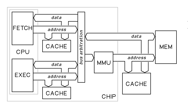
Typical modern computers contain multiple caches plus a memory management unit. An instruction cache or I cache holds only instructions, speeding the fetch phase of the fetch-execute cycle. A data cache or D cache holds only operands, and serves to speed the execute phase of the fetch-execute cycle. Sometimes, instead of separate I and D caches, these are combined into a single on-chip cache, the L1 cache. In addition, it is common to find an L2 cache that is outside the processor chip, and there are systems that use an L3 cache; sometimes each memory chip has a separate L3 cache. The cache levels L1 and L2 are counted moving from the processor toward memory. Thus, a complete system might be even more complex than that shown here:
|
In the above diagram, the central processor has two separate interfaces to memory, each with its own cache; this is possible because most modern processors are pipelined, so that the next instruction is fetched while its predecessor is executed. If the execute phase of one instruction involves a memory reference, for example, when the instruction is a load or store instruction, the processor tries to perform this load or store in parallel with the instruction fetch. Because of the separate caches for the fetch and execute stages of the pipeline, it is possible that these two memory cycles will indeed take place in parallel. Only when both caches have a miss will the bus arbitration logic have to select between the two memory references, allowing the execute memory reference to go first, and then allowing the next instruction fetch.
Exercises
a) In the last figure above, identify the various caches according to type (I cache, D cache, L1 cache, L2 cache, L3 cache, etc). Note that there may be multiple caches of one kind and none of some other kind. Also note that multiple names may be applicable to some of the caches.
b) In the last figure above, if the mapping function performed by the memory management unit is changed, the contents of some of the caches must be erased. Which caches, and what makes their contents invalid.
c) Suppose input/output devices are connected to the same address and data busses as the main memory. Explain why the presence of cache memory causes problems when a program attempts to read the device registers. Hint: Consider the impact of caches on a polling loop that repeatedly tests the device ready bit in a memory-mapped device register.
Our goal here is to show how a cache can be built from a small, fast random-access memory and a bit of auxiliary logic. If our memory address space allows a single 32-bit word of memory to be selected by a 30 bit address, this means that the main memory could be up to a gigaword, 230 words. Here, we will assume a cache of only 32 kilowords, 215 words. This is not an unusual size for the L2 cache on a modern processor. Of course, we will also assume that our small memory is much faster than main memory. If one memory cycle on main memory takes 50 nanoseconds, it is reasonable to rely on an L2 cache that has a 5 nanosecond cycle time. The internal L1 cache or the I cache and D cache might have cycle times of 0.5 nanoseconds in the same system.
One way to imagine the function of such a cache is in algorithmic terms. We can imagine, with each each reference to main memory, that the central processor calls either the read or write routine on the cache. These routines begin by searching the cache. If they find the desired data, they use the data from the cache, while if they do not, they update the cache to hold the desired data from main memory. The following code outlines this view:
unsigned int address_table[cachesize];
unsigned int value_table[cachesize];

unsigned int cache_read( unsigned int address )
{
    int i;
    for (i = 0; i < cachesize; i++) {
        if (address_table[i] == address) { /* hit */
            return value_table[i]
        }
    }
    /* miss */
    i = replacement_policy( 0, cachesize );
    address_table[i] = address;
    value_table[i] = RAM_read( address );
    return value_table[i];
}
|
void cache_write( unsigned int address, unsigned int value )
{
    int i;
    for (i = 0; i < cachesize; i++) {
        if (address_table[i] == address) { /* hit */
	    value_table[i] = value;
            RAM_write( address, value );
            return;
        }
    }
    /* miss */
    i = replacement_policy( 0, cachesize );
    address_table[i] = address;
    value_table[i] = value;
    RAM_write( address, value );
    return;
}
|
The above algorithmic view of what a cache does is only correct up to a point. There are two important caveats: First, the replacement policy that determines which location in the cache gets used is completely unspecified. How this policy operates has a big impact on the performance of the cache. Second, the algorithmic description uses a sequential search to find cache hits; this cannot possibly perform adequately. An effective cache must perform this search in parallel.
The easiest way to build a cache completely determines the replacement policy. For our small 32K cache, consider what happens if we use 15 bits of the 30 bit main memory address to select a word in the cache. As a result, each word in the cache can hold the value of one out of 32K different words in main memory. For each particular word in main memory, there is exactly one word of cache that can be associated with it. At any instant, that word of the cache will be associated with just one of 32K different words in main memory, so we must store 15 bits of the memory address with that word in order to remember which particular word in main memory it mirrors.
The result of this argument is that each entry in our small cache must holds 15 bits of address along with the 32 bits of data. We call these extra bits the cache tag. The following schematic describes the core of our cache memory:
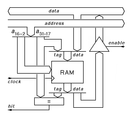
|
The logic shown here has one output to the cache controller, hit, indicating that the addressed word in the cache's memory has a tag that matches the contents of the address bus. The cache controller for this cache must produce 2 control signals, clock, to indicate when a new data word and its tag should be stored in the cache's memory, and enable to control when a data word from the cache's memory should be put on the data bus.
The job of the cache controller is to clock new data into the cache's internal memory whenever there is valid data on the data bus along with a valid address on the address bus, and, in response to a hit that occurs when there is a read request from the processor, to put the cache's data on the data bus, cutting the memory cycle short.
This cache design is called a write-through cache because it does nothing to accelerate write cycles. Write-back cahces are more complex, but their payoff is lower because most memory cycles issued by most processors are for read operations. Write-back caches allow the CPU to continue as if a write to main memory had been completed as soon as the cache gets a copy of the value written. The cache is responsible for completing this write at a later time. As a result, the cache controller a cache controller for a write-back cache must be able to initiate a write to memory independently of the CPU. The I cache that handles only instruction fetches need not support write cycles at all, and when a system has both L1 and l2 caches, it is fairly common for one of these to be a simple write-through cache.
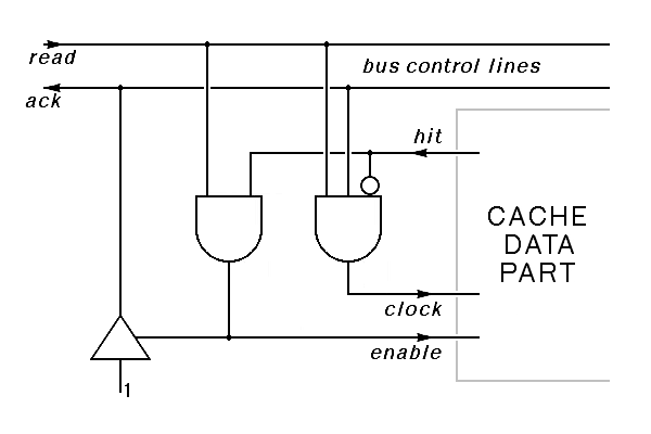
A control system for this cache must connect with the bus control lines. Here, we will assume that there is a read line that is asserted when the processor attempts to read from memory, and an ack line asserted by memory in response. The read signal indicates that a valid address is already on the address lines, and the ack line indicates that the data from memory is valid. The cache itself will assert the ack line when there is a hit. If we ignore write cycles, for example, because the cache is serving a read-only memory or because the cache is being used as an I cache, no other control signals are involved, and the full cache controller looks like this:
|
Note here that both the cache controller and the memory can drive the ack signal. If neither drives this signal, it is false. We show this using a bus driver on the cache controller; this driver provides no output if it is not enabled, and provides a constant output of one if it is enabled.
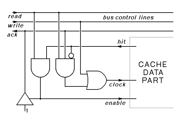
Extending this cache controller to make a write-through cache is not difficult. The primary new requirement is that the cache should record the value written whenever there is a write to memory. To support write operations, we must extend our set of bus control lines by adding a write signal that goes true when a valid address and the data to be written are both present on the bus. Again, we will assume that the memory responds to this with an ack signal to acknowledge completion of the write.
|
Both the cache controller and the bus interface for a write-back cache are more complex, since such a cache must be able to initiate memory cycles independently from the CPU. In effect, the cache controller for such a cache is an independent but very simple processor. It responds to bus cycles initiated by the central processor, but like a peripheral device's direct memory access interface, it can also initiate its own memory cycles.
Exercises
d) If the address lines are switched in the cache above, so that the most significant bits of the address are used to select a word from the cache's memory and the least significant bits of the address are stored as the tag, the cache will still work, but poorly. It would work as well as the original if addresses issued by the processor were random, but it works very poorly for typical programs. Why?
e) The random access memory used in the cache shown here has a 15-bit memory address. How big is each word of this memory? (Hint: It is not the same as the word size of the computer!)
The simplest memory management model involves breaking the memory address space of the processor into a sequence of fixed size pages, while the actual physical memory is broken into equal-sized page frames. In such a paged virtual memory system, any page used by the program can be stored in any page frame of physical memory, and the function of the memory management unit is to substitute the correct frame number into the physical address, when given a page number from the virtual address.
The data structure used for this substitution has been called the page table or the memory map. The memory management unit operates by using the page number from the virtual address to select a page-table entry, and then forming the physical address, in part, from the frame-number field of the page-table entry. The part of the address that remains unchanged through this translation is the word-in-page field, or the byte-in-page field, in cases where memory is byte addressable.
In programming notation, the function of the memory management unit is as follows:
constant unsigned int pagesize = (1 << bits_in_bytefield);

unsigned int physical_address( unsigned int virtual_address )
{
	unsigned int address_in_page = virtual_address & (pagesize - 1);
	unsigned int page_number = virtual_address >> bits_in_bytefield;
	unsigned int frame_number = page_table[ frame_number ];
	return (frame_number << bits_in_bytefield) | address_in_page;
}
|
The simplest memory management units store the entire page table inside a very small, very fast memory that is part of the memory management unit itself. For example, the Digital Equipment Corporation PDP-11 had a virtual address that was 16 bits in length, and a physical address that was 18 bits in length. The first memory management unit sold with this machine had a structure based on the following outline:
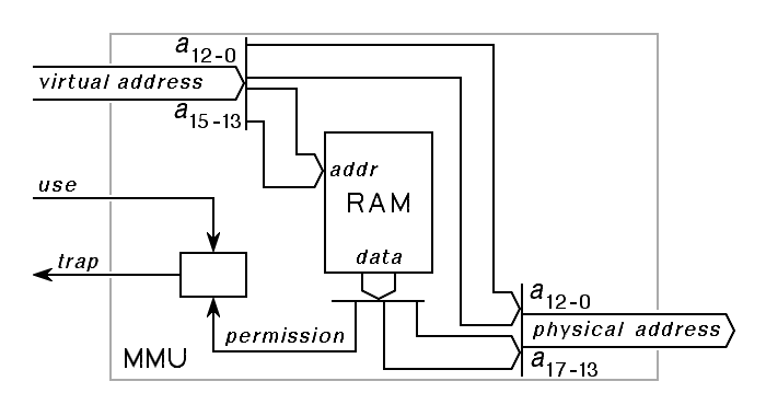
|
On the PDP-11, the top 3 bits of the 16-bit virtual address were used to select one of 8 entries in the page table inside the memory management unit. The simplest way to use each page table entry was to use that entry to provided the top 5 bits of the 18-bit physical address. This solved two problems: First, it quadrupled the amount of main memory that could be attached to the machine, from 64K bytes to 256K bytes, and second, by changing the page table with each change from one running application to another, it was possible to give each application a protected memory address space, thus controlling the damage that could be done by a malfunctioning application.
| 15 | 14 | 13 | 12 | 11 | 10 | 09 | 08 | 07 | 06 | 05 | 04 | 03 | 02 | 01 | 00 |
| page | byte in page | ||||||||||||||
The term page is generally used when talking about the view of memory seen by the program. Thus, each virtual address contains three bits used to specify the page being addressed, with the lower bits of the address specifying the byte or word within that page. In contrast, when speaking about physical addresses, we generally use the term page frame or just frame to refer to a region of memory exactly big enough to hold one page of a program's address space. As a result, the fields of a physical address are generally referred to as the frame field and the word-in-frame or byte-in-frame field.
| 17 | 16 | 15 | 14 | 13 | 12 | 11 | 10 | 09 | 08 | 07 | 06 | 05 | 04 | 03 | 02 | 01 | 00 |
| frame | byte in frame | ||||||||||||||||
Another detail shown in the diagram for the PDP-11 memory management unit is a trap-request output from the memory management unit to the central processor. The memory management unit will request a trap if the use being made of a virtual address does not match the permissions associated with the referenced page. Each page-table entry contains not only the frame number associated with the given page, but also the permissions or access rights for the page. When the central processor issues a memory address, it also indicates the use it intends to make of that address, for example, whether a read or a write operation is intended. The permission field of the page table indicates, for each page, what uses are permitted, and the trap logic inside the memory management unit compares the use proposed with the permissions granted.
The operating system is responsible for setting the access rights associated with each page. Pages containing variables are usually marked as read-write, while the pages containing instructions and constants are marked read-only. Some machines permit more subtle distinctions such as allowing pages that contain only instructions and no constants to be marked execute-only, pages containing only constants and not instructions to be marked read-only, and pages containing a mixture to be marked read-execute. Generally, when the operating system matches the access rights closely with the needs of the program, program malfunctions will be detected sooner and misbehaving programs will have a smaller likelihood of doing any harm before they are caught.
The figures given here do not show how the page table is loaded into the memory management unit. In the case of the PDP-11, the 8 registers holding the page table within the memory management unit were treated as input-output device registers, so the operating system could load them the same way it did input and output.
Exercises
f) The PDP-11 had byte addressing and a 16-bit word. Therefore, the virtual address has a word-in-page field and a byte-in-word field. Redraw the figures for the PDP-11 address layouts to show this detail.
g) How many bytes were there in a PDP-11 page, as described above.
h) The real PDP-11 memory management unit did not divide the address space into fixed-size pages, but rather, into 8 variable-sized segments, where segments could be any number of 32-byte chunks in size, up to a maximum given by the size of the byte-in-segment field of the virtual address. Each segment could begin with any 32-byte chunk of physical memory, with the remainder of the segment occupying consecutive 32-bit chunks. Each page-table entry, therefore, contained the base address of a segment, in chunks, and the size of that segment, in chunks. Show the layout of the virtual and physical addresses.
i) Given the details given in the previous problem, how many bits are there in each segment-table entry? Give a possible layout for these bits.
j) Given the details given in the previous problems, plus the fact that the memory management unit used an adder to add the chunk-in-segment field of the virtual address to the base-chunk-address from the page table, give a diagram for the data flow through the memory management unit.
As already mentioned, the most elementary use of the memory management unit is to provide each application that shares a computer with a separate virtual address space. As a result, each application is unable to address any memory other than that specifically given to that application by the operating system. Without a memory management unit, programming errors in an appliction can potentially damage other applications or event he operating system itself, while with a memory management unit, the consequences of programming errors or mailicious programmers are strictly limited. As such, memory management units are essential components secure computer systems and fault-tolerant computer systems.
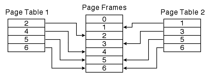
Once each application has been given its own address space, a number of things become possible. Each application can be given a virtual address space that appears entirely private, as if each application were running on a different computer, or the address spaces can be arranged to selectively share memory. It is the possibility of selective sharing of information that makes a single computer running multiple applications more interesting than a number of separate computers isolated from each other. To share a page between two virtual address spaces, all we need to do is edit the page table entry for that page in each address space so that it refers to the same page frame. The contents of that frame will then be visible in both address spaces, as is the case with frames 5 and 6 shown in the figure below.
|
An appropriate memory management unit can also allow a small machine to address a large main memory. For example, the maximum possible memory on the original PDP-8 sold by Digital Equipment Corporation in 1965 was 4K 12-bit words. As customers developed applications needing more memory, DEC offered an optional memory management unit was that allowed the PDP-8 to address 32K 12-bit words.
The first version of the DEC PDP-11 sold in 1970 supported a maximum memory of 48K 8-bit bytes; the remainder of the 64k address space was used for memory mapped input/output. It is noteworthy that the 16-bit PDP-11 was intended to replace the 12-bit PDP-8, and 48K 8-bit bytes have the same number of bits as 32K 12-bit words. Again, as customers developed applications needing more memory, DEC offered models with a memory management unit supporting a larger physical memory.
Intel's 8080 microprocessor, introduced in the mid 1970s, allowed a maximum memory of 64k bytes. Intel made several changes when they moved from the 8080 to the 8086, but one of the most important was a rudimentary memory management unit allowing this second-generation 16-bit microprocessor to address more than 64K of memory.
The final reason for using a memory management unit is actually the first one that was commercially exploited. A memory management unit plus an appropriate trap handler plus a large slow memory such as a disk can be used to create a virtual address space bigger than the main memory. At any particular time, most of the pages of the virtual address space are stored on disk, while only those pages currently being used are stored in page frames in main memory. When the program attempts to address a page that is not in main memory, the memory management unit forces a trap, called a page fault. This scheme is called demand-paged virtual memory because pages of the application program are transferred between main memory and disk on demand instead of being transferred in anticipation of demand.
The structure of a page-fault trap handler is typically discussed, in some detail, in elementary operating systems courses. In short, the page-fault trap handler must find a free frame in main memory, typically by evicting some page from main memory to disk, and then it must read the page needed by the application from disk into this free frame. Having done this, it can update the page table to reflect the new locations of each of these pages and then return to the application program.
This use of virtual memory requires that the trap hardware have one very special property: When the memory management unit requests a trap, the saved processor state must be the state immediately prior to fetching the instruction that caused the trap. Without this, the return from trap would not properly retry the instruction that caused the trap. If the hardware does not automatically save the right state, the software can sometimes undo the effects of a partially executed instruction.
Consider the question "how many times was the program counter incremented before the trap occurred?" On the Hawk, the answer depends on the opcode, and without knowing how many times the program counter was incremented, we cannot know which memory location contains the opcode of the instruction that caused the trap. On the Hawk, the hardware solves this problem for us by setting the TPC register to the address of the first halfword of the instruction that caused the trap.
There is a second problem. If all the page frames in RAM are currently in use, which page frame should be empitied so it can hold the page the user needed? This is determined by the trap handler's page replacement policy. As with cache replacement, the particular policy adopted can have a big effect on performance. The worst case is to replace the page that the program is about to use, perhaps on the very next instruction, while the best case is to replace that page that the program will not use for the longest possible time into the future.
Lacking a crystal ball for predicting the future, realistic page replacement policies must estimate the likelihood that pages will be needed in the future by looking at history. The best practical policy is to replace that page that was least recently used. This policy, called LRU replacement, requires the memory management unit to maintain records of the most recent use of each page frame. Few memory management units do this, so most real systems rely on approximations of this.
Exercises
k) The Hawk memory management unit records the address of the instruction that caused the trap into the TPC register. Suppose, instead, that it recorded the PC register at the instant of the trap. To allow demand-paged virtual memory under this new scheme, we can reserve a new field of the processor status word to hold how many times the program counter was incremented by the current instruction. First, how big would this field be on the Hawk, and second, what would the trap handler do with the value of this field.
l) The Hawk uses memory-mapped input-output. How can the memory-management unit be used to prevent an application program from directly accessing any input-output devices?
m) If the page table itself is stored in main memory, how can we use the memory management unit to prevent application programs from changing the page table? Failure to do this would prevent virtual memory from being used to achieve any security goals.
The simple memory management unit structure of the PDP-11
has a big problem: It does not scale well.
For a 16-bit virtual address
with only 8 pages per address space, it was easy to build a very fast
8-entry random access memory and incorporate this in the memory management
unit. Machines with 256 pages in the virtual address space, using an 8-bit
page field, have been built using this basic approach, but we cannot simply
scale this up for use on a 32-bit machine. Consider the layout of the bits
in a Hawk virtual address, a layout typical of many 32-bit
processors.
| 31 | 30 | 29 | 28 | 27 | 26 | 25 | 24 | 23 | 22 | 21 | 20 | 19 | 18 | 17 | 16 | 15 | 14 | 13 | 12 | 11 | 10 | 09 | 08 | 07 | 06 | 05 | 04 | 03 | 02 | 01 | 00 |
| page | word in page | byte | |||||||||||||||||||||||||||||
Storing the page-table for this virtual address format inside the memory management unit would require that the small fast memory there contain 220 entries, about a million. Furthermore, loading a new page table into this memory would require updating all of these million entries, something we cannot afford to do each time the machine switches from one application to another.
The solution to this problem involves the use of cache technology. Instead of storing the entire page table within the memory management unit, we only store that part of the page table that is currently relevant. For historical reasons, this special purpose cache is called a translation lookaside buffer, sometimes abbreviated TLB. So long as the program only references page table entries that are in the TLB, the processor runs at full speed. When the program references a new page, however, we have what is called a TLB fault.
Remarkably, the memory management units built in the 1960s and 1970s generally handled TLB faults entirely in hardware, stopping the execution of the program while the memory management unit reached into main memory for the appropriate page-table entry. This requires a memory management unit controller with direct memory access and some processing power. It was only in the 1980s that the designers of what came to be called reduced-instruction-set-complexity architectures or RISC architectures discovered that it was frequently quite reasonable to let software handle TLB faults.
Before we delve into the details of the Hawk memory management unit, it is important to understand that, in general, memory management unit of a computer may be turned off. When the computer is first started, the memory management unit is off, and it is up to the software to turn it on after the memory maps are properly established and the appropriate trap service routines are ready to catch memory management unit traps. In the case of the Hawk, the most significant bit of the level field of the processor status word, bit 31, determines whether or not the memory management unit is on. If this bit is one, the memory management unit is active. If it is zero, the memory management unit is off and virtual addresses and physical addresses are the same.
Each field in the Hawk translation lookaside buffer consists of 45 bits, although we will always view this as two 32-bit words with several unused bits. Using terminology from cache memory, the first word of each entry holds the tag field, a 20-bit page number. The second word holds the data associated with this, a 20-bit frame number plus 5 bits giving the access rights that protect it.
| 31 | 30 | 29 | 28 | 27 | 26 | 25 | 24 | 23 | 22 | 21 | 20 | 19 | 18 | 17 | 16 | 15 | 14 | 13 | 12 | 11 | 10 | 09 | 08 | 07 | 06 | 05 | 04 | 03 | 02 | 01 | 00 |
| page number | |||||||||||||||||||||||||||||||
| frame number | C | R | W | X | V | ||||||||||||||||||||||||||
If the page number issued by the central processing unit does not match the page number of any entry in the translation lookaside buffer, the memory management unit will request a trap. If the page number issued by the central processing unit matches some entry, the corresponding frame number is substituted into the address in order to create the physical address. The physical address is not used until the permissions from the matching entry are checked against the use the processor is proposing. If the translation lookaside buffer is marked as invalid, or if the proposed operation on memory is not permitted, the memory management unit forces the central processing unit to trap, aborting the execution of the current instruction.
| bit | purpose | |||
|---|---|---|---|---|
| C | -- | cache enabled | ||
| R | -- | load permitted | ||
| W | -- | store permitted | ||
| X | -- | instruction fetch permitted | ||
| V | -- | entry valid |
Note that each translation lookaside buffer entry has one special bit, the cache enable bit C that determines whether results from any cache memory will be accepted. This bit should be set, by the operating system software, for all pages in memory that are stored in normal random access memory, but it should be reset for pages of the address space that reference device registers. When a program attempts to read from a device register, it wants the actual contents of that register and not something remembered from the past by a cache sitting between the central processor and the device.
Conceptually, we may describe the behavior of the Hawk MMU by an algorithm, but as with the algorithms we've used to describe the behavior of caches, the Hawk algorithm uses a linear search where the real MMU would use a parallel compare operation. Also note that the size of the Hawk translation lookaside buffer, TLB_size in the following, is hidden from the programmer. All the programmer needs to know is that the translation lookaside buffer holds at least two entries and probably more.
constant unsigned int bits_in_pagesize_field = 12;
constant unsigned int pagesize = 1 << bits_in_bytefield; /* 4096 */

unsigned int physical_address( unsigned int virtual_address )
{
    int i;
    unsigned int address_in_page = virtual_address & (pagesize - 1);
    unsigned int page_number = virtual_address >> bits_in_bytefield;

    for (i = 0; i < TLB_size; i++) {
	if (TLB[i].page_number == page_number) { /* hit */
            unsigned int frame_number = TLB[i].frame_number;
            return (frame_number << bits_in_pagefield) | address_in_page;
	}
    }
    /* miss */
    raise PAGE_FAULT;
}
|
When the memory management unit requests a trap, it is reported to the operating system as a bus trap, which is to say, control is transferred to location 1016 and the memory management unit is turned off because the level field of the processor status word is set to zero. The trap service routine for the bus trap can then determine the cause of the trap by examining the following resources:
The trap handler may read this using the CPUGET instruction, and the CPUSET instruction may be used to change this register.
The trap handler may write this register using the CPUSET instruction, doing so places the contents of TMA and MMUDATA in some entry of the translation lookaside buffer. The software has no control over what entry is used, but there is a guarantee that the MMU will never contain more than one TLB entry for any particular page number. Each memory management unit will implement some workable replacement policy.
The design of the Hawk memory management unit allows a trap handler written for a small memory management with a crude replacement politcy to continue working if the memory management unit is upgraded to one with a big translation lookaside buffer and a sophisticated replacement policy. The trap handler never needs to know size of the translation lookaside buffer or the replacement policy being used. All that matters from the software perspective is that there are enough entries in the translation lookaside buffer to allow program execution, and that the memory management unit hardware will not use the worst possible replacement policy.
The worst possible replacement policy would be to replace the most recently used entry in the translation lookaside buffer. In most cases, this entry will be the one that is most likely to be used next, since consecutive instructions are frequently executed from the same page. Either random replacement or first-in, first-out replacement would be better, but the best possible TLB replacement policy is the same policy that works best with cache memory and demand paged virtual memory. The best possible TLB replacement policy would be ro replace the least recently used translation lookaside buffer entry, but as with cache and virtual memory systems, typical hardware will only approximate this.
Exercises
n) On the Hawk, access to the page table used by the memory management unit is through the CPUSET and CPUGET instructions. Why is it imortant to prevent applications programs from accessing these instructions?
o) Look at the algorithmic descriptions given for the cache-write function and for the Hawk memory management unit and write a corresponding algorithmic description for the operation of writing the MMUDATA register. As with the cache-write function, you can assume a function called replacement-policy that handles that issue.
This chapter is incomplete and will be expanded at some point with an example MMU trap handler