8. Arithmetic and Logic.
Part of
CS:2630, Computer Organization Notes
|
19th century logicians, most notably George Boole, identified the basic operators of what we know know as Boolean algebra, and, or and not. These are the familiar operators used in Boolean expressions in programming languages as well as being among the basic operators of the logic that philosophers have studied for millenia. What logicians like Boole did was bring these into the realm of mathematics by showing that they formed an algebra in just the way that addition and subtraction on the integers do.
Our goal is to examine enough Boolean algebra see how basic arithmetic operations can be done using only Boolean operations. This allows us to study how the arithmetic unit of a computer works. We will not discuss how Boolean operations are implemented in hardware, but will accept, on faith, that it is possible. Thus, we will ignore tranistors and electronics.
Boolean logic operates on the values true and false, and it was George Boole who recognized that if true is represented by the value one and false is represented by the value zero, we can think of or as being like addition, where adding zero does nothing. Similarly, and as like multiplication, where multiplying by zero gives zero and multiplying by one does nothing.
Based on these observations, Boole proposed that we use the symbols for arithmetic operators to stand for logic operators. So, in Boolean notation, a+b means a or b, and ab means a and b. This notation is still widely used, with only one minor change. Where Boole used the minus sign to mean not, modern logicians tend to use an overbar, so modern logicians write either a or ¬a instead of –a to mean not a. One other symbol has come into common use in Boolean algebra, the use of a⊕b to mean a exclusive-or b. This is true if a is true or b is true, but not both.
The field of Switching theory emerged before World War II, motivated by the use of complex systems of electromechanical relays in telephone exchanges. This field applies Boolean logic to practical engineering problems. With the development of electronic calculators and then computers, switching theorists quickly moved into the center of key aspects of computer design.
Electrical engineers refer to hardware devices that perform the functions of Boolean operators as logic gates. Each physical logic gate has connections for a power supply as well as connections for inputs and outputs. The term gate comes from the analogy with a path crossing a fence. Data travels down the path through the gate when it is open, but data on a second path controls the gate, opeing it at some times, closing it at others.
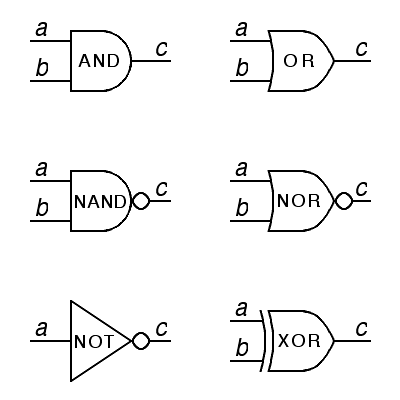
Electrical engineers have a long tradition of using graphical notations to do their design work, and by the late 1960's, MIL-STD-806, promulgated by the US Air Force, came to be widely accepted as the standard graphical notation for Boolean logic. This is well suited to the problem of describing the Boolean logic used in computer design and more generally in switching circuits. The basic elements of this notation are given below. In this notation, inputs are shown on the left and outputs are shown on the right. A schematic diagram shows the interconnection of inputs and outputs as lines between the symbols for the individual gates; these are usually called wires, even if the actual hardware uses conductive traces on silicon or a printed circuit board.
|
|
| inputs | the output c | ||||||
| a | b | and | or | nand | nor | not | xor |
| a b | a + b | a b | a + b | a | a ⊕ b | ||
| 0 | 0 | 0 | 0 | 1 | 1 | 1 | 0 |
| 0 | 1 | 0 | 1 | 1 | 0 | 1 | |
| 1 | 0 | 0 | 1 | 1 | 0 | 0 | 1 |
| 1 | 1 | 1 | 1 | 0 | 0 | 0 | |
In addition to the conventional Boolean operators and, or and not, engineers quickly introduced two new operators, nand and nor. These correspond to and and or with their results inverted by a not operator, as indicated in the algebraic notation for Boolean logic by an overbar over the expression. These were introduced largely because the simplest amplifiers used in digital logic perform the not function, and a typical hardware implementation of the and or or function produces an output that must be amplified before it is used as an input to another logic operator.
The triangle symbol is an old symbol for an amplifier in electronic schematics, and it is still used in this way in some schematic diagrams for logic circuits, standing for a gate (called a buffer) with inputs and outputs that are equal. The small circle on the output of the nand, nor and not gates indicates logical negation. This is usually placed on the output of the gate, but occasionally, you will see this little circle placed on an input in order to indicate the presence of an inverter or not gate built into that input.
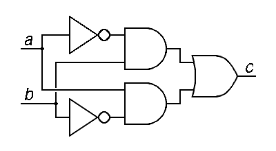
The exclusive-or operator is also given a special symbol in this schematic notation, but not because it is a primitive operator or easy to build in hardware. In fact, the exclusive-or operator is difficult to build, requiring hardware equivalent to 4 nand operators, but it is common in arithmetic units. The following shows one of many ways to build exclusive-or from simple gates:
| ||
| c = a ⊕ b = (a b) + (a b) | ||
One way to describe exclusive-or is to say that the exclusive or of two inputs is true if only one input is true while the other is false. The figure above corresponds exactly to the this explanation.
Some standard notational conventions make schematics easier to read. First, inputs are usually on the top or left, and outputs are usually on the bottom or right. Thus, information usually flows from top to bottom or left to right. Second, when wires cross, this is shown by drawing one wire as if it hops over or tunnels under the other, while where wires are connected, a dot (historically representing a screw) is used to show the connection. To avoid ambiguity, connections are usually drawn with lines meeting to form a T, while crossings form an X.
Historically, engineering students bought templates to help draw logic gate symbols. If you do draw them freehand, note that the key features that distinguish an or symbol from an and symbol are that the or has a curved input side and a point on the output side, while the and has a straight input side and a perfect half-circle for the output side. Both symbols can be drawn inside a square box.
a) Consider the logic diagram given above for an exclusive-or gate built from and, or and not gates. What function does this compute if the 2 not gates are replaced by a single nand to combine the a and b inputs and passes its result to the two inputs originally served by separate not gates.
b) Two 1-bit binary numbers can be compared for equality with an exclusive-or gate and one more gate to give an output of 1 if the numbers are equal and 0 if they differ. Draw the schematic diagram for a solution to this problem and give an equation in Boolean logic notation.
Any algebra is characterized by a set of values and a set of functions over those values. In common algebra, we start with a set of numbers and the arithmetic operators. There are many numerical algebras, depending on whether we start with real numbers, complex numbers or something else. In Boolean algebra, our set has just two values, true and false, operated on by the Boolean operators. The basic laws of this algebra define the behavior of these operators. Many of these laws look very much like the laws of numerical algebra, but a few are different:
| zero | a + 1 = 1
a 0 = 0 |
| identity | a + 0 = a
a 1 = a |
| commutative | a + b = b + a
a b = b a |
| associative | (a + b) + c = a + (b + c)
(a b) c = a (b c) |
| distributive | a (b + c) = a b + a c
a + b c = (a + b) (a + c) |
The first and last laws above do not hold for arithmetic. Numerical algebras have only one zero, but Boolean algebra has two values that can be described as zeros. Not only does anding anything with 0 give 0, but oring anything with 1 gives 1. In numerical algebra, multiplication distributes over addition, but not visa versa. In Boolean algebra, and distributes over or and or distributes over and. We can prove this using a truth table:
| a | b | c | bc | a+bc | a+b | a+c | (a+b)(a+c) |
| 0 | 0 | 0 | 0 | 0 | 0 | 0 | 0 |
| 0 | 0 | 1 | 0 | 0 | 0 | 1 | 0 |
| 0 | 1 | 0 | 0 | 0 | 1 | 0 | 0 |
| 0 | 1 | 1 | 1 | 1 | 1 | 1 | 1 |
| 1 | 0 | 0 | 0 | 1 | 1 | 1 | 1 |
| 1 | 0 | 1 | 0 | 1 | 1 | 1 | 1 |
| 1 | 1 | 0 | 0 | 1 | 1 | 1 | 1 |
| 1 | 1 | 1 | 1 | 1 | 1 | 1 | 1 |
This is a proof by exhaustion. All combinations of a, b and c are shown. The column headed a+bc gives one side of the distributive law, while the column headed (a+b)(a+c) gives the other. The fact that the values in these columns are equal proves the law. The other columns show terms that were used to compute the key columns.
The exclusive-or operator is not covered by the basic laws because it is considered to be a derived operator. It is possible to prove from these laws that the following identities hold for it:
| identity | a ⊕ 0 = a |
| inverse | a ⊕ 1 = a |
| commutative | a ⊕ b = b ⊕ a |
| associative | (a ⊕ b) ⊕ c = a ⊕ (b ⊕ c) |
We can prove the above laws using algebra, starting with the algebraic definition of exclusive-or in terms of and, or and not. Algebraic proofs can be hard because you have to find a path through a maze of algebraic substitutions. With only two Boolean values, it can be easier to use an exhaustive proof expressed as a truth table.
Augstus De Morgan discovered are two laws of Boolean algebra that have no precedent in numerical algebra, De Morgan's laws. These complete the story of the symmetry of and and or that is apparent in the basic laws given above.
| a + b | = | a b | ||
| a b | = | a + b |
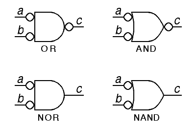
We can use De Morgan's laws to create new symbols for some of the basic logic gates:
|
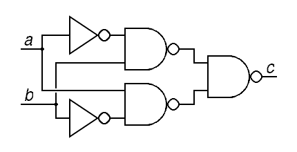
Remember, bubbles on the inputs and outputs of gate symbols mean not. Under De Morgan's laws, an and gate with inverters on its inputs and outputs acts like an or gate, so an and gate with inverters on its inputs only is a nor gate. We can use this to redraw the schematic diagram for an exclusive-or gate with three nand gates instead of the cascade of and and or gates in the original:
|
c) Construct the truth table to prove that and distributes over or.
d) Use a truth table to prove both versions of De Morgan's laws.
e) Write out the algebraic formula for a ⊕ b using only the nand and not operators.
f) Here is a fragment of C code. Rewrite it using De Morgan's Laws to replace the or operator with an and operator. Express the result as simply and compactly as possible:
if ((a < 0) || (a > 9)) error( "out of bounds" );
Each bit of a binary number can obviously be associated with a Boolean value, and George Boole's convention that 1 is used to represent true and 0 is used to represent false apply naturally to this problem. Thus, we can think of the 32-bit binary number a as being composed of a vector of Boolean values a0 to a31, where the subscripts incicate the power of two in the place-value system.
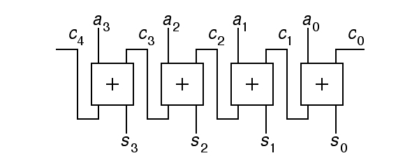
Given numbers represented as arrays of bits, how can we build hardware to do arithmetic operations? To start with, how can we increment a number? It is useful to start with a review how to do this by hand. We add one to the least significant digit. If the result is greater than the radix, we carry by adding one to the next digit. This may cause yet another carry. It is all done with a operation at each digit that computes the output value for this digit and also the carry to be added to the next digit. In schematic terms, this is:
|
In the above diagram, the 4-bit addend a is incremented by c0 to produce the 4-bit sum s. The carry bits ci violate our standard convention for the direction of data-flow in a schematic, left to right and top to bottom, because we have allowed our convention for writing numbers to force the least significant bit to be shown on the right. The carry input to the entire incrementer is c0. If this is zero, the sum s will equal the addend a, while if it is one, s will usually equal a+1. The intermediate carry bits c1 to c3 hold the carry out of one stage of the incrementer and into the next. The final carry bit, c4 holds the carry out of the adder; if this is one, the input a must have been 1111 and the output s is 0000, an unsigned overflow.
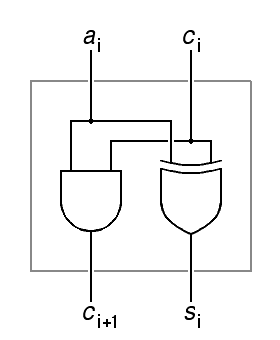
The logical operation performed at each bit position in the above incrementer in the box marked with a plus is fairly simple. There are two inputs, ai and ci, and two outputs, si and ci+1, so the truth table for this function will have 4 rows and two output columns. Here it is:
| inputs | outputs | ||
| ai | ci | ci+1 | si |
| 0 | 0 | 0 | 0 |
| 0 | 1 | 0 | 1 |
| 1 | 0 | 0 | 1 |
| 1 | 1 | 1 | 0 |
The above truth table was filled in by summing the bits
in the input row and then recording this sum, as a binary
number, in the output row. The least significant bit of the output is the
sum output for that bit position, while the most significant bit of the
output is the carry into the next bit position. With this table,
it is easy to compare each output column with the outputs of the various
standard Boolean functions. From this, we see that
ci+1 is just the logical and of
ai and ci, and that
si is the exclusive or of
ai and ci. This leads to the
following gate-level design for each digit of the incrememter:
| ||||
| ci+1 | = | ai ci | ||
| si | = | ai ⊕ ci | ||
The increment logic described above is exactly that used in low-performance computers. The problem with this logic is that the time to increment a number grows linearly with the number of bits. That is, incrementing n bits takes O(n) time. For computers built this way, a 32-bit computer would run at half the speed of a 16-bit machine. Even Charles Babbage knew this was a bad idea, and he coined the term carry anticipation to refer to logic to quickly predict the carry into a stage of the increment or add circuitry. Since the late 1950s, we have used circuits that allow increment or add operations to be done in O(log n) time using a carry lookahead tree.
g) Work out the truth table for decrementing a binary number, with inputs ai (a bit of the input) and bi (the borrow input to that bit) and outputs bi+1 and di (the decremented output). Follow through and give a gate-level schematic for one bit of a decrementor. Note: Assume bi is true when one is to be taken from ai and false when no change is to be made.
h) From algebra, a-1 is -((-a)+1), and in the two's complement system, -x is x+1. Combining these allows us to build a decrementor from an incrementer and some added inverters. Show the logic diagram for this.
We can design an adder using the same approach we used for an incrementer. As with the incrementer, addition involves propagating carries from one digit to the next, but instead of a single input, we have two inputs, the addends, which we will call a and b. Addition is commutitive, so we can call them both addends. Older texts sometimes refer to one as the addend and the other as the augend to distinguish between the number that is augmented and the number added to it. At the top level, a 4-bit adder looks like this:
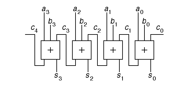
|
The truth table for one bit of an adder is very similar in form to that for
one bit of the incrementer, but with 3 inputs instead of 2. As with the
truth table for the incrementer, we can read each two-bit output row as a
binary number giving the number of one bits in the corresponding
inputs, but now, our sums run from zero to three instead of from zero to two.
Here is the table for the adder:
| ||||||||||||||||||||||||||||||||||||||||||||||||||||
The first 4 rows of the above table output are the same as the table
for the increment function, but the whole table is
messy enough that it is hard to see how to get the outputs from
the inputs.
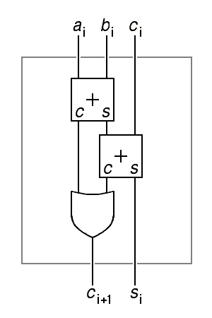
Focusing only on the sum output si, this output is one only when an odd number of ones appear in the corresponding input row. Note that, so long as any input to the table is zero, the output is the exclusive or of the other two inputs, and if any input to the table is one, the output is the opposite. This implies that si=ai⊕bi⊕ci There is no need for parentheses because exclusive or is associative.
The carry output ci+1 is more complex, but it is not difficult to determine that ci+1=aibi+aici+bici.
Another ad-hoc reasoning path leads to the fact that an adder can be made from two incrementers plus an additional or to combine the carry outputs. Because of this, the increment circuit is sometimes called a half adder and the three-input adder is distinguished from the incrementer by calling it a full adder.
|
Ad-hoc design is slow and labor intensive unless luck grants you
the right flash of inspiration. If we want to build interesting
computers without waiting for inspiration, we need a systematic
approach to designing logic circuits that implement arbitrary Boolean
functions. Switching theory, a field that began to develop in the
1920's motivated by the development of the dial telephone system, provides
a general methodology
for converting any truth table to a logic circuit to compute the Boolean
function described by that table:
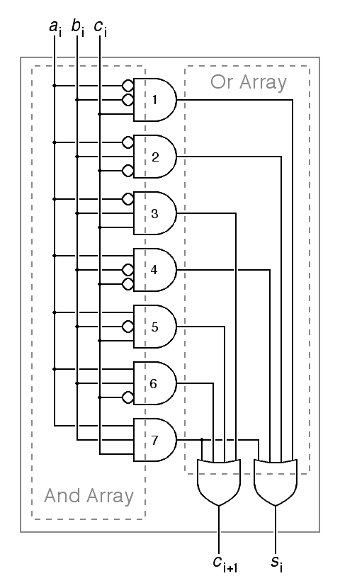
Except in trivial cases, this methodology produces results that are optimal in speed, assuming a constant delay per gate, but it does not minimize the number of logic gates. However, the designs that emerge from this methodology are good starting points for optimization. It is also worth noting that this methodology can be used to create a circuit that behaves as a read-only memory (ROM), with an address as input and the corresponding data as output.
Once a circuit has been designed using this brute-force method, we can optimize it by combining rows whenever those rows have identical outputs but inputs that differ in exactly one bit position. Where this is true, that input can be ignored and a single and gate with one less input can be substituted for the two. If we combine all combinable rows that differ in the first bit position, and then combine all combinable rows that differ in the second bit position and so on, this produces an optimal circuit. We will not emphasize optimization here.
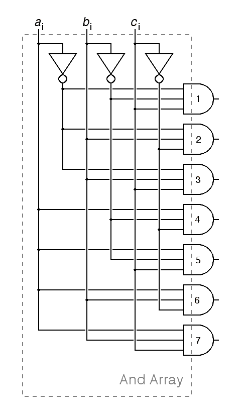
We have used a common notational abbreviation in the adder circuit below. Instead of cluttering the diagram with inverters, bubbles on the inputs to the and gates show which inputs are inverted. You can read the binary representation of the row number from the inputs of each and gate by starting at the top and reading bubbles as zeros and un-inverted inputs as ones. The and array is redrawn on the right below without this abbreviation.
|
|
i) Show the truth table for a subtractor that computes d=a-b, with borrow signals connecting the digit positions. The top-level schematic view of this subtractor should be identical to the top-level schematic view of the adder. Also, what function does it compute when the least significant borrow input is true?
j) Draw out the gate-level schematic view of an adder given above, using explicit not gates instead of bubbles on the inputs to the and gates. Note: This can be done with exactly 3 inverters, since no input needs inversion more than once.
It is time to ask how the condition codes are derived from the outputs of an adder built as discussed above. The N condition code is the simplest. Because the Hawk is a two's complement machine, we can treat the most significant bit of the sum as the sign and copy it into the N condition code.
The Z condition code should be set if every bit in the sum is zero. Equivalently, Z should be reset if any bit in the sum is nonzero. The equivalence of these two follows from De Morgans laws. As a result, we can use a multi-input nor gate to combine all of the bits of the sum to produce the Z condition code.
The C bit is simply the carry out of the most significant bit of the adder. V, the overflow bit, is more difficult. There are several equivalent ways to compute V. There is an overflow if the signs of the addends are the same but the sign of the result is different. This require two sign comparisons. Alternatively, there is an overflow if the carry into the sign position differs from the carry out of the sign bit. This takes just one exclusive-or gate:
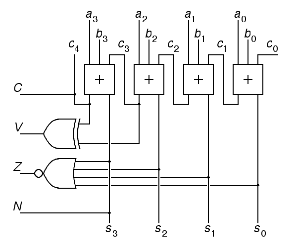
|
The simplicity of the condition code logic demonstrated above explains why it has become so dominant in the design of binary computers since it was first introduced with the PDP-11 in 1970. Many earlier machines had just a carry bit, plus the ability to test any register for zero or negative.
The above schematic violates our standard drawing convention that data should flows from left to right and top to bottom. Here, we have the carry input c0 on the right and all 4 condition code outputs on the left. We do this because we always write numbers with the least significant bit on the right and all but one condition code reports on things that concern the most significant bit, while the carry in is an input to the least significant bit.
k) The text mentions that there is an overflow when the signs of the operands are the same but the sign of the result is different. Express this as a truth table, assuming a 4-bit adder, so the inputs are a3, b3 and s3. Reduce this truth table to logic gates using the systematic brute-force method.
l) Draw the part of the schematic diagram for the derivation of the condition codes that pertains to the Z condition code, but using an and gate and, if necessary, some inverters.
We can use a simple adder for the arithmetic involved in indexed addressing, but what we really want at the heart of our CPU is a general purpose block of logic that can both add subtract, as well as performing other operations. This is called an arithmetic logic unit or ALU because it can perform Boolean logic as well as arithmetic.
How do we take our adder and extend it so that it can do other operations? First, note that an adder can subtract if we negate one operand, and negation is easy in two's complement arithmetic. To negate a two's complement number, invert each bit, taking the one's complement, and then add one to the result. Furthermore, the carry in to the adder can be used to add that extra one. So we subtract by adding the one's complement with a carry in of one.
Next, recall that a ⊕ 0 = a while a ⊕ 1 = a; this means that exclusive or can be used to select between a logical value and its inverse. This leads to the following design for an adder-subtractor:
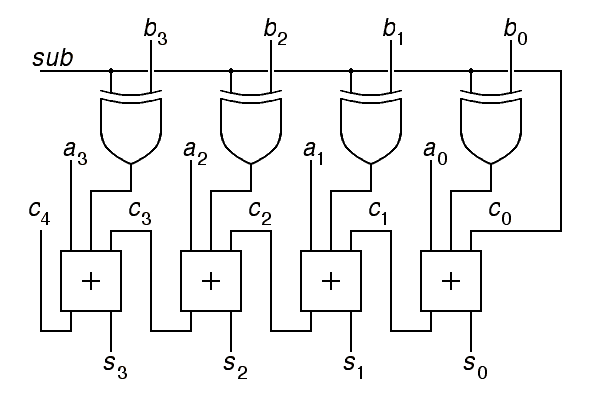
|
Here, if the sub input is zero, the b inputs are not changed
by the exclusive-or gates and c0, the carry in
to the adder, is zero. As a result, the circuit computes the sum
s=a+b+0 in this case.
On the other hand, if the sub input is one, the b inputs are inverted by the exclusive-or gates and c0 is one, so the adder computes s=a+b+1. Given that we are using two's complement representations, so that b+1=–b, we can conclude that the circuit computes the difference s=a–b in this case.
We need more. The set of operations supported by C, for example, include not just addition and subtraction, but a much longer list that includes and, or and exclusive or as well a shift operators and more advanced arithmetic operators such as multiply and divide. We will ignore multiply, divide and floating point for now, and concentrate on the simpler operations.
Modern hardware designers have created highly optimized arithmetic logic units to perform these additional operations, where the same circuitry that does addition and subtraction also does logical operations. We will examine those, but first, we will look at a simpler approach based on a general-purpose circuit that can be used to select between its data inputs depending on the value of a control input. For example, we can use such a circuit to select between logical operators and arithmetic, and within the logical operators, to select between and, or and exclusive-or.
A logic circuit that has its output equal to exactly one of several data inputs depending on a control input is called a multiplexer, abbreviated MUX. This term dates to the late 19th century, when the idea of multiplexing multiple telegraph circuits onto one telegraph line was developed. At the sending end of the line, a multiplexer would combine the signals from multiple telegraph keys onto the wire, and at the receiving end, a demultiplexer separated them.
In the context of digital logic, a multiplexer with n data inputs must have log2n control inputs. For our example arithmetic-logic unit, we need a multiplexer with 4 data inputs and 2 control inputs. The Hawk CPU, with 15 registers, needs several 16-input multiplexers for register selection, each using a 4-bit register number as a control input. We will not give full truth tables for these larger multiplexers, but the truth table for a multiplexer with 2 data inputs d0 and d1 and one control input c is as follows:
| inputs | output | ||
| c | d0 | d1 | f |
| 0 | 0 | 0 | 0 |
| 0 | 0 | 1 | 0 |
| 0 | 1 | 0 | 1 |
| 0 | 1 | 1 | 1 |
| 1 | 0 | 0 | 0 |
| 1 | 0 | 1 | 1 |
| 1 | 1 | 0 | 0 |
| 1 | 1 | 1 | 1 |
The above truth table reduces to a logic circuit with just 4 gates:
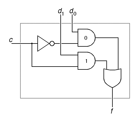
|
|
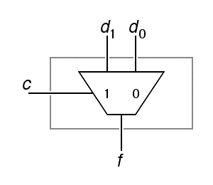
| f = (d0 c) + (d1 c) | |
The shorthand notation on the right above includes labels inside the "funnel" to indicate the value of the control input that selects the corresponding data input. Usually, the "funnel" is oriented to pass data from top to bottom or from left to right, following our conventions for data flow in schematics, but the funnel shape clearly indicates the direction of data flow so, as with the conventional symbols for and and or, this symbol can be used in nonstandard orientations without ambiguity. Here is the gate-level design for a 4-input multiplexer:
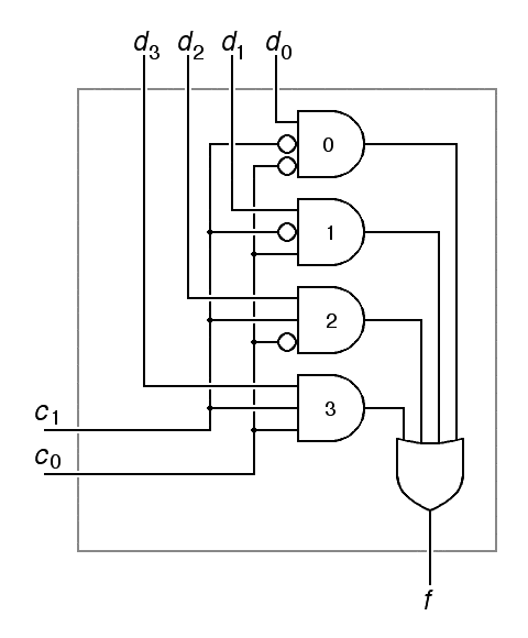
|
|
| f = (d0 c1 c0 ) + (d1 c1 c0 ) + (d2 c1 c0 ) + (d2 c1 c0 ) | |
Here, we have used an abbreviated notation for
inverters. While there are 4 inversion bubbles in the figure, we would only
use 2 inverters to build this circuit, one per control input.
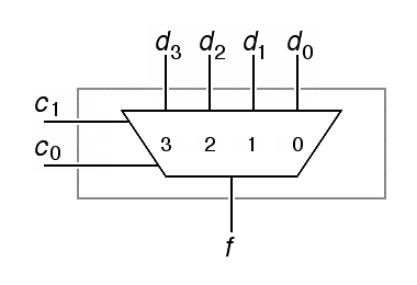
In the abbreviated notation to the right, the reader can infer
that the labels 0, 1, 2 and 3 inside the multiplexer symbol correspond to
00, 01, 10, and 11 on the control lines, where c1
is the most significant bit and c0 is the least significant.
The funnel shape used for multiplexors is sometimes used for other functions that combine multiple inputs into one output. If there is no other label and the inputs are labeled with values of the control input, you can assume it is a multiplexer.
We now have the parts we need to build a simple arithmetic logic unit that combines an adder-subtractor with three simple logic gates using a multiplexer. Here, we have drawn just one one bit of this unit, with data inputs ai, bi and ci, data outputs si and ci+1, add-subtract control input f2, and two more control inputs f1 and f0 for the multiplexer.
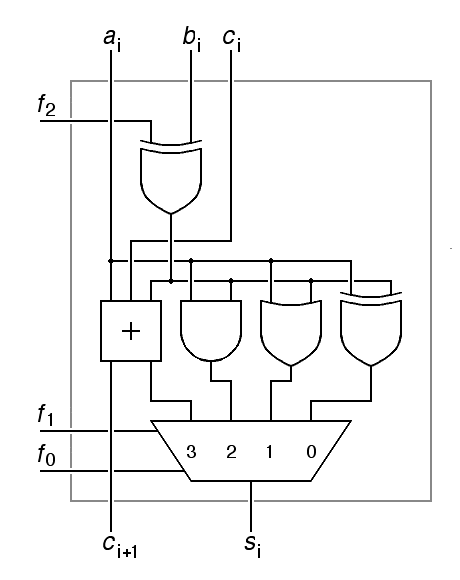
|
We call this a bit slice of the arithmetic logic unit. The full arithmetic logic unit for a machine like the Hawk would require a total of 32 such bit slices. Desigers of CPUs frequently break up the design into bit slices. Nowdays, each bit slice might occupy a rectangular space on the surface of an integrated circuit. In early computers, each bit slice was frequently packaged as one or more printed circuit boards. On the original PDP-8 computer, for example, the CPU was made of 12 bit slices, each of which occupied two printed circuit boards.
High-performance arithmetic logic units are rarely constructed as shown here because of two major categories of optimization. First, the carry path through the arithmetic logic unit is almost always carefully optimized, so that carry propagation from the carry in to the least significant bit to the carry out from the most significant bit is far faster than is suggested by the designs given here. This frequently involves carry anticipation logic.
Second, we can make the adder itself compute the and, or and exclusive-or functions so that there is no need for a multiplexer for function selection. We do this by adding auxiliary inputs to the adder that control which terms are active. The net result is that the arithmetic logic unit is reduced to an exclusive-or gate per bit for selecting between addition and subtraction, plus a slightly augmented adder that does all arithmetic and logic. A typical modified adder is shown below.
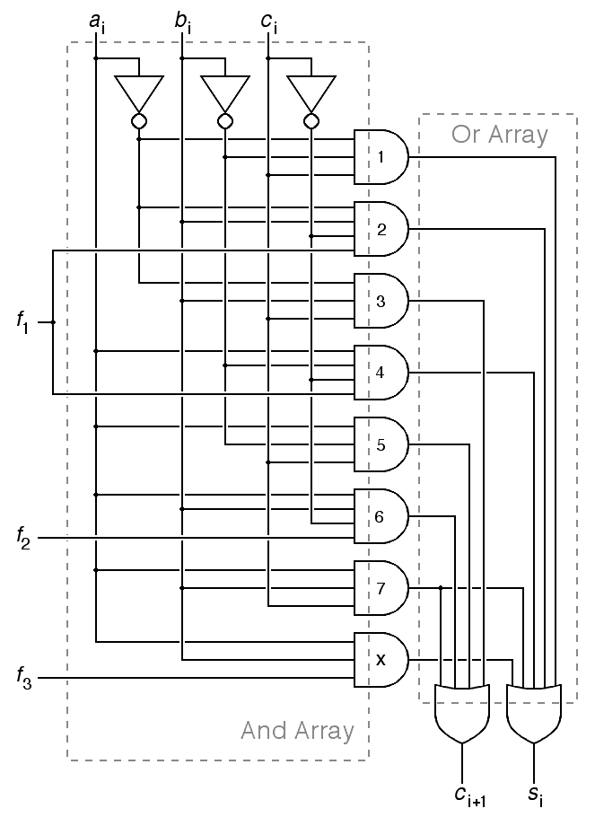
|
Auxiliary input f1 has been added to control and gates 2 and 4 of the adder, and input f2 has been added to control and gate number 6. A single gate has been added to the and array in the modified adder, labeled x in the figure. This gate is enabled by the auxiliary input f3. If f1 and f2 are both set true and f3 is set false, the modified adder behaves exactly like the original.
If f2 is false and there is no carry in to the least significant bit of the adder, all of the carry bits will be zero, and as a result, so long as f1 is true, the adder will compute the exclusive or of the a and b inputs. Setting f3 true converts exclusive or to or, and setting f1 false while holding f3 true converts or to and.
m) In the adder-subtrtactor, the carry output means carry, exactly, when the circuit is used for addition. When the circuit is used for subtraction, however, the situation is a bit muddy. What is the value of the carry output when the high bit of the subtractor outputs a borrow request and when the high bit of the subtractor does not output a borrow request?
n) Naive students frequently assume that the borrow signal should flow from more significant places in the subtractor to less significant places because when you borrow one, you take one from a more significant place and give it to a less significant place. Explain why this is wrong.
o) Redraw the 2-input multiplexer given above with only nand gates (this is an application of De Morgan's laws).
p) Another way to build a 4-input multiplexer is with a binary tree of 2-input multiplexers. Draw the schematic diagram for this tree, and then estimate the number of and, or and not gates required to build this tree and compare this with the 7 gates required to build the 4-input multiplexer directly. Can you give corresponding figures for an 8-input multiplexer built using this binary tree approach compared to an 8-input multiplexer built directly?
q) The bit-slice of an arithmetic logic unit given above has 3 control inputs, f2, f1 and f0. Therefore, it can compute 8 distinct fuctions of its a and b inputs. List them, and then go throught the Hawk instruction set and figure out which Hawk register-to-register instructions can be implemented with each. Ignore memory-reference instructions; indexing on Hawk uses a separate adder.
r) Show how to build an exclusive-or gate from a 2-input multiplexer plus an inverter. Use the trapezoid symbol to expres your result.
s) Show how an adder can be built from two 8-input multiplexers, one to compute the sum and one to compute the carry. Hint: All of the data inputs should be constants, either 0 or 1.
t) In the adder modified to perform logic, there are 3 control inputs, 4 control inputs, f1, f2 f3 plus c0, the carry into the least significant bit. Make a table of the 16 combinations, and for each table entry, identify whether that combination is potentially useful and if so, what function the modified adder computes.
In addition to arithmetic and logic operations, most computers and many programming languages support shift operators. In languages descended from C, such as C++ and Java, these are >> meaning shift right and << meaning shift left. The effects of these operators are illustrated below, starting with the value 8:
| expression | value | |
|---|---|---|
| binary | decimal | |
| i | 00001000 | 8 |
| i >> 1 | 00000100 | 4 |
| i >> 2 | 00000010 | 2 |
| i >> 3 | 00000001 | 1 |
| i << 1 | 00010000 | 16 |
| i << 2 | 00100000 | 32 |
| i << 3 | 01000000 | 64 |
Shifting is included in the instruction set for two reasons: First, it allows moving bits around, for example, to extract successive bits from a word for transmission over a serial data line, or to pack multiple 4-bit data items into a word. The second reason is apparent when you examine the decimal equivalent of the binary values in the example above. Shifting left c places multiplies by 2c and shifting right c places divides by 2c (rounding the result down).
A hardware device that takes an n-bit number as input and shifts that number c places is called a shifter. A shifter for an n-bit word can be made from n multiplexers, where the number of inputs per multiplexer determines how many different values of the shift-count c the shifter can handle. Here is a 4-bit right shifter:
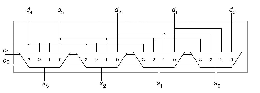
|
We have made a notational compromise above. In order to save space, we have drawn the control inputs as if they passed under the multiplexers. This is commonly done in schematic diagrams, but only when the input signals in question are distributed identically to all of the parts to which they connect. That is the case here.
The shifter shown above computes s = d >> c; that is, it shifts its 4-bit input right from 0 to 3 places. This poses an interesting question: What value should be "shifted into" the output for bits that were not part of the input number? In the above, this value is provided by an auxiliary input, d4. For left-shift operations, the usual answer is to shift zeros in from the left, so that the result is the result you would expect for multiplication by 2c.
For right-shift, there are two useful answers. First, we could shift in zeros, as with left-shift; in this case, the result will be the correct result for division by a power of two, assuming that the input number was treated as an unsigned integer. This is called a logical right shift or an unsigned right shift. The other alternative is to shift in copies of the sign bit. For the 4-bit shifter shown above, this would involve connecting the d4 input to d3. In this case, if the input is a two's complement binary number, the output will be the correct two's complement result for division by a power of two, with one very important exception: If the quotient is not exact, that is, if there is a nonzero remainder after division, the result will be rounded to the next lower integer instead of being rounded toward zero. As a result, -5>>1 is -3, not -2. This is called an arithmetic right shift or a signed right shift.
Note that In C and C++, when you declare a variable to be of type int and then apply the >> operator to it, this implies a signed right shift, while if you declare the variable to be of type unsigned int and then apply the same operator, this implies an unsigned shift. In contrast, in Java, where the built-in integer type is signed and there is no way to declare unsigned integers, the there are two distinct right-shift operators, >> and >>> for the signed and unsigned shifts.
The Hawk machine has both left and right shift operators, and right shifts are available in both signed and unsigned form. One feature of the Hawk machine that separates it from many other machines is that the shift operators are combined with a variant of the add instruction, so that one instruction can both shift a number and add to it. The Hawk instructions for this are ADDSL, ADDSR and ADDSRU (the latter being the unsighed right shift). To accomodate these shifted versions of the add operation, there is a right-shifter on the output of the Hawk arithmetic logic unit and a left-shifter on one of the inputs of the Hawk arithmetic logic unit.
As with the discussion of arithmetic logic units, the design of shifters used in real computers is frequently more complex than that given here. The primary problem with the approach given here is that a 32-bit shifter with a 4-bit shift-count would take 32 multiplexers with 16 inputs each. In designing computers, it is common to avoid using extravagant amounts of silicon for rarely used functions, and in the case of shifters, the solution is to use a shift tree, also called a barrel shifter, where one stage of the shifter shifts only a short distance, say 0 to 3 bits using a 2-bit shift count, while the next stage shifts in multiples of 4, again using a 2-bit shift count. As a result, we can achieve exactly the same shift function with 64 4-input multiplexers instead of 32 16-input multiplexers.
u) Draw the diagram for a 4-bit left shifter able to shift from zero to three places.
v) Draw the diagram for a 4-bit right shifter composed of a cascade of two levels using 2-bit multiplexers at each level, where the top level shifts either 0 places or 2 places, while the second level shifts either 0 places or 1 place. Make sure to label the inputs and outputs so that they are exactly compatable with the 4-bit shifter illustrated above.
w) Explain how the Hawk EXTB instruction is implemented using eight 4-input multiplexers. What bits of what register(s) are used to control these multiplexers? What bits of what register(s) are used as inputs to these multiplexers? What bits of what register(s) take the outputs of these multiplexers.
We have shown that addition and subtraction operators can be built in hardware using a number of logic gates proportional to the word size. One bit of an adder can be built from about 12 and, or and not gates. Adding an exclusive-or gate to one input of this adder converts it to an adder-subtracter, at a cost of 4 primitive gates to build the exclusive or. To make it do logic operations, we need to add just one and gate. Adding these up gives us the cost of one bit slice of an arithmetic logic unit, and multiplying by the 32 bits per word gives us an estimate for the number of gates in the Hawk arithmetic-logic unit.
| Modified Adder | 13 | ||
| exclusive or to make adder-subtractor | + 4 | ||
| Total gates per bit | 17 | ||
| word size | × 32 | ||
| Estimated gate count for the Hawk ALU | 544 | ||
This estimate, 544 gates, supports only the simple arithmetic and logic operations. To get the left and right shift operations, we must add two shift networks, one for left shift and one for right shift. The Hawk shift instructions take shift counts between 1 and 16, so each shift network can be made of either 32 16-input multiplexers or 64 4-input multiplexers. We will assume the latter.
| 4-input multiplexer | 7 | ||
| word size | × 32 | ||
| gates per 32-bit 4-way shifter | 224 | ||
| 2 layers of shifters | × 2 | ||
| gates per 32-bit 16-way shifter | 448 | ||
| need both left and right shifts | × 2 | ||
| Total gates for the Hawk shift network | 896 | ||
Adding the 896 gates for the two shift networks to the 544 gates in the arithmetic logic unit gives us an estimate for the total complexity of the Hawk's arithmetic and shifting hardware: 1,440 and, or and not gates. This estimate ignores the cost of optimizing for fast carry propagation and it ignores all of the control unit.
x) Estimate the cost, in gates, of the ALU-shifter for a 16-bit digital signal processor chip (a DSP), assuming it supports only the following shift operations: byte-swap, left shift one place, right shift one place, or don't shift at all. These options apply to the output of the ALU.
y) The accounting above assumed the use of two layers of 4-way multiplexers to construct a shift network that could shift from 0 to 15 places. How does the result differ if you assume 4 layers of 2-way multiplexers to do this job.